PI5C3390SX, PI5C3394Q, PI5C3400 Selling Leads, Datasheet
MFG:PERICOM Package Cooled:SOP D/C:08+/09+

PI5C3390SX, PI5C3394Q, PI5C3400 Datasheet download

Part Number: PI5C3390SX
MFG: PERICOM
Package Cooled: SOP
D/C: 08+/09+


MFG:PERICOM Package Cooled:SOP D/C:08+/09+
PI5C3390SX, PI5C3394Q, PI5C3400 Datasheet download
MFG: PERICOM
Package Cooled: SOP
D/C: 08+/09+

Want to post a buying lead? If you are not a member yet, please select the specific/related part number first and then fill the quantity and your contact details in the "Request for Quotation Form" on the left, and then click "Send RFQ".Your buying lead can then be posted, and the reliable suppliers will quote via our online message system or other channels soon.
TOP
PDF/DataSheet Download
Datasheet: PI5A100
File Size: 525000 KB
Manufacturer: PERICOM [Pericom Semiconductor Corporation]
Download : Click here to Download
PDF/DataSheet Download
Datasheet: PI5A100
File Size: 525000 KB
Manufacturer: PERICOM [Pericom Semiconductor Corporation]
Download : Click here to Download
PDF/DataSheet Download
Datasheet: PI5C3400
File Size: 58326 KB
Manufacturer: PERICOM [Pericom Semiconductor Corporation]
Download : Click here to Download
Pericom Semiconductor's PI5C series of logic circuits are produced in the Company's advanced 0.8 micron CMOS technology, achieving industry leading speed grades.
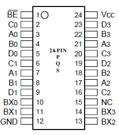
The PI5C3400 is a 4-bit, 4-port bus switch with individual exchanges designed with a low ON resistance (5W) allowing inputs to be connected directly to outputs. The bus switch creates no additional propagational delay or ground bounce noise. The switches are turned ON by the Bus Enable (BE) input signal, and the Bus Exchange (BX0BX3) input signals offer individual bit swapping of the AB and CD signal pairs. This exchange configuration allows bit swapping of buses in systems.
Above which the useful life may be impaired. For user guidelines, not tested.
Storage Temperature ............................................................ 65°C to +150°C
Ambient Temperature with Power Applied ............................40°C to +85°C
Supply Voltage to Ground Potential (Inputs & Vcc Only) ..... 0.5V to +7.0V
Supply Voltage to Ground Potential (Outputs & D/O Only) .. 0.5V to +7.0V
DC Input Voltage ..................................................................... 0.5V to +7.0V
DC Output Current ............................................................................... 120 mA
Power Dissipation .................................................................................... 0.5W
Note:
Stresses greater than those listed under MAXIMUM RATINGS may cause permanent damage to the device. This is a stress rating only and functional operation of the device at these or any other conditions above those indicated in the operational sections of this specification is not implied. Exposure to absolute maximum rating conditions for extended periods may affect reliability.

Price: 4-6 USD
MT58L64L18CT-10 TQFP100

Price: 5-6.5 USD
DL-7140-211M laser tube

Price: 4-5 USD
74LVC74APG - IC FLIP FLOP D-Type POS-EDG DUAL 14TSSOP

Price: 6.5-8 USD
CYPRESS - Clock Synthesizer with Differential CPU Outputs

Price: 0.284-0.286 USD
PI5V330QEX Pericom Multiplexer Switch ICs

Price: 1-2 USD
IGBT power module, Single switch, 1200 V, Collector-emitter voltage, 430A

Price: 1-2 USD
a-Si TFT-LCD, NEC, 228.096Hmm, 560V

Price: 0.124-0.2 USD
PC354N1T - Mini-flat Package, AC Input Type Photocoupler - Sharp Electrionic Components

Price: 0.177-0.178 USD
RL1210JR51-XX-BL - Thick Film Chip Resistor Low Ohmic - TAITRON Components Incorporated

Price: 0.053-0.055 USD
STPS140A - POWER SCHOTTKY RECTIFIER - STMicroelectronics

Price: 1.45-1.5 USD
STA013 - MPEG 2.5 LAYER III AUDIO DECODER - STMicroelectronics

Price: 0.073-0.075 USD
SMBJ5347B - 5 Watt Surface Mount Silicon Zener Diodes - Micro Commercial Components
