Want to post a buying lead? If you are not a member yet, please select the specific/related part number first and then fill the quantity and your contact details in the "Request for Quotation Form" on the left, and then click "Send RFQ".Your buying lead can then be posted, and the reliable suppliers will quote via our online message system or other channels soon.
The SST31LF041/041A/043/043A devices are a 512K x8 CMOS flash memory bank combined with a 128K x8 or 32K x8 CMOS SRAM memory bank manufactured with SST’s proprietary, high performance SuperFlash technology. The SST31LF041/041A/043/043A devices write (SRAM or flash) with a 3.0-3.6V power supply. The monolithic SST31LF041/041A/043/043A devices conform to Software Data Protect (SDP) commands for x8 EEPROMs. Featuring high performance Byte-Program, the flash memory bank provides a maximum Byte-Program time of 20 µsec. The entire flash memory bank can be erased and programmed byte-by-byte in typically 8 seconds, when using interface features such as Toggle Bit or Data# Polling to indicate the completion of Program operation. To protect against inadvertent flash write, the SST31LF041/041A/ 043/043A devices have on-chip hardware and Software Data Protection schemes. Designed, manufactured, and tested for a wide spectrum of applications, the SST31LF041/041A/043/043A devices are offered with a guaranteed endurance of 10,000 cycles. Data retention is rated at greater than 100 years.
The SST31LF041/041A/043/043A operate as two independent memory banks with respective bank enable signals. The SRAM and Flash memory banks are superimposed in the same memory address space. Both memory banks share common address lines, data lines, WE# and OE#. The memory bank selection is done by memory bank enable signals. The SRAM bank enable signal, BES# selects the SRAM bank and the flash memory bank enable signal, BEF# selects the flash memory bank. The WE# signal has to be used with Software Data Protection (SDP) command sequence when controlling the Erase and Program operations in the flash memory bank. The SDP command sequence protects the data stored in the flash memory bank from accidental alteration.
The SST31LF041/041A/043/043A provide the added functionality of being able to simultaneously read from or write to the SRAM bank while erasing or programming in the flash memory bank. The SRAM memory bank can be read or written while the flash memory bank performs Sector- Erase, Bank-Erase, or Byte-Program concurrently.
All flash memory Erase and Program operations will automatically latch the input address and data signals and complete the operation in background without further input stimulus requirement. Once the internally controlled Erase or Program cycle in the flash bank has commenced, the SRAM bank can be accessed for Read or Write.
The SST31LF041/041A/043/043A devices are suited for applications that use both nonvolatile flash memory and volatile SRAM memory to store code or data. For all system applications, the SST31LF041/041A/043/043A devices significantly improve performance and reliability, while lowering power consumption, when compared with multiple chip solutions.
The SST31LF041/041A/043/043A inherently use less energy during Erase and Program than alternative flash technologies. When programming a flash device, the total energy consumed is a function of the applied voltage, current, and time of application. Since for any given voltage range, the SuperFlash technology uses less current to program and has a shorter Erase time, the total energy consumed during any Erase or Program operation is less than alternative flash technologies.
The monolithic ComboMemory eliminates redundant functions when using two separate memories of similar architecture; therefore, reducing the total power consumption. The SuperFlash technology provides fixed Erase and Program times, independent of the number of Erase/Program cycles that have occurred.
Therefore the system software or hardware does not have to be modified or de-rated as is necessary with alternative flash technologies, whose Erase and Program times increase with accumulated Erase/Program cycles. The SST31LF041/041A/043/043A devices also improve flexibility by using a single package and a common set of signals to perform functions previously requiring two separate devices.
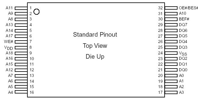
To meet high density, surface mount requirements, the SST31LF041/043 device is offered in 40-lead TSOP package and the SST31LF041A/043A device is offered in 32-lead TSOP package. See Figures 1 and 2 for the pinouts.
SST31LF041 Maximum Ratings
Operating Temperature . . . . . . . . . . . . . . . . . . . . . . . . . . . . . . . . . . . . . . . . . -20°C to +85°C Storage Temperature . . . . . . . . . . . . . . . . . . . . . . . . . . . . . . . . . . . . . . . . . -65°C to +150°C D. C. Voltage on Any Pin to Ground Potential . . . . . . . . . . . . . . . . . . . . . .. . -0.5V to VDD+0.5V Transient Voltage (<20 ns) on Any Pin to Ground Potential . . . . . . . . . . .. . -1.0V to VDD+1.0V Voltage on A9 Pin to Ground Potential . . . . . . . . . . . . . . . . . . . . . . . . . . . . . . . . -0.5V to 13.2V Package Power Dissipation Capability (Ta = 25°C) . . . . . . . . . . . . . . . . . . . . . . . . . . . . 1.0W Surface Mount Lead Soldering Temperature (3 Seconds) . . . . . . . . . . . . . . . . . . . . . . . 240°C Output Short Circuit Current1. . . . . . . . . . . . . . . . . . . . . . . . . . . . . . . . . . . . . . . . . . . . .. 50 mA 1. Outputs shorted for no more than one second. No more than one output shorted at a time.
SST31LF041 Features
• Monolithic Flash + SRAM ComboMemory – SST31LF041/041A: 512K x8 Flash + 128K x8 SRAM – SST31LF043/043A: 512K x8 Flash + 32K x8 SRAM • Single 3.0-3.6V Read and Write Operations • Concurrent Operation – Read from or write to SRAM while Erase/Program Flash • Superior Reliability – Endurance: 100,000 Cycles (typical) – Greater than 100 years Data Retention • Low Power Consumption: – Active Current: 10 mA (typical) for Flash and 20 mA (typical) for SRAM Read – Standby Current: 10 µA (typical) • Flash Sector-Erase Capability – Uniform 4 KByte sectors • Latched Address and Data for Flash • Fast Read Access Times: – SST31LF041/043 Flash: 70 ns SRAM: 70 ns – SST31LF041A/043A Flash: 300 ns SRAM: 300 ns • Flash Fast Erase and Byte-Program: – Sector-Erase Time: 18 ms (typical) – Bank-Erase Time: 70 ms (typical) – Byte-Program Time: 14 µs (typical) – Bank Rewrite Time: 8 seconds (typical) • Flash Automatic Erase and Program Timing – Internal VPP Generation • Flash End-of-Write Detection – Toggle Bit – Data# Polling • CMOS I/O Compatibility • JEDEC Standard Command Set • Packages Available – 32-lead TSOP (8 x 14 mm) SST31LF041A/043A – 40-lead TSOP (10 x 14 mm) SST31LF041/043
SST31LF041 Connection Diagram
SST31LF041A General Description
The SST31LF041/041A/043/043A devices are a 512K x8 CMOS flash memory bank combined with a 128K x8 or 32K x8 CMOS SRAM memory bank manufactured with SST’s proprietary, high performance SuperFlash technology. The SST31LF041/041A/043/043A devices write (SRAM or flash) with a 3.0-3.6V power supply. The monolithic SST31LF041/041A/043/043A devices conform to Software Data Protect (SDP) commands for x8 EEPROMs. Featuring high performance Byte-Program, the flash memory bank provides a maximum Byte-Program time of 20 µsec. The entire flash memory bank can be erased and programmed byte-by-byte in typically 8 seconds, when using interface features such as Toggle Bit or Data# Polling to indicate the completion of Program operation. To protect against inadvertent flash write, the SST31LF041/041A/ 043/043A devices have on-chip hardware and Software Data Protection schemes. Designed, manufactured, and tested for a wide spectrum of applications, the SST31LF041/041A/043/043A devices are offered with a guaranteed endurance of 10,000 cycles. Data retention is rated at greater than 100 years.
The SST31LF041/041A/043/043A operate as two independent memory banks with respective bank enable signals. The SRAM and Flash memory banks are superimposed in the same memory address space. Both memory banks share common address lines, data lines, WE# and OE#. The memory bank selection is done by memory bank enable signals. The SRAM bank enable signal, BES# selects the SRAM bank and the flash memory bank enable signal, BEF# selects the flash memory bank. The WE# signal has to be used with Software Data Protection (SDP) command sequence when controlling the Erase and Program operations in the flash memory bank. The SDP command sequence protects the data stored in the flash memory bank from accidental alteration.
The SST31LF041/041A/043/043A provide the added functionality of being able to simultaneously read from or write to the SRAM bank while erasing or programming in the flash memory bank. The SRAM memory bank can be read or written while the flash memory bank performs Sector- Erase, Bank-Erase, or Byte-Program concurrently.
All flash memory Erase and Program operations will automatically latch the input address and data signals and complete the operation in background without further input stimulus requirement. Once the internally controlled Erase or Program cycle in the flash bank has commenced, the SRAM bank can be accessed for Read or Write.
The SST31LF041/041A/043/043A devices are suited for applications that use both nonvolatile flash memory and volatile SRAM memory to store code or data. For all system applications, the SST31LF041/041A/043/043A devices significantly improve performance and reliability, while lowering power consumption, when compared with multiple chip solutions.
The SST31LF041/041A/043/043A inherently use less energy during Erase and Program than alternative flash technologies. When programming a flash device, the total energy consumed is a function of the applied voltage, current, and time of application. Since for any given voltage range, the SuperFlash technology uses less current to program and has a shorter Erase time, the total energy consumed during any Erase or Program operation is less than alternative flash technologies.
The monolithic ComboMemory eliminates redundant functions when using two separate memories of similar architecture; therefore, reducing the total power consumption. The SuperFlash technology provides fixed Erase and Program times, independent of the number of Erase/Program cycles that have occurred.
Therefore the system software or hardware does not have to be modified or de-rated as is necessary with alternative flash technologies, whose Erase and Program times increase with accumulated Erase/Program cycles. The SST31LF041/041A/043/043A devices also improve flexibility by using a single package and a common set of signals to perform functions previously requiring two separate devices.
To meet high density, surface mount requirements, the SST31LF041/043 device is offered in 40-lead TSOP package and the SST31LF041A/043A device is offered in 32-lead TSOP package. See Figures 1 and 2 for the pinouts.
SST31LF041A Maximum Ratings
Operating Temperature . . . . . . . . . . . . . . . . . . . . . . . . . . . . . . . . . . . . . . . . . -20°C to +85°C Storage Temperature . . . . . . . . . . . . . . . . . . . . . . . . . . . . . . . . . . . . . . . . . -65°C to +150°C D. C. Voltage on Any Pin to Ground Potential . . . . . . . . . . . . . . . . . . . . . .. . -0.5V to VDD+0.5V Transient Voltage (<20 ns) on Any Pin to Ground Potential . . . . . . . . . . .. . -1.0V to VDD+1.0V Voltage on A9 Pin to Ground Potential . . . . . . . . . . . . . . . . . . . . . . . . . . . . . . . . -0.5V to 13.2V Package Power Dissipation Capability (Ta = 25°C) . . . . . . . . . . . . . . . . . . . . . . . . . . . . 1.0W Surface Mount Lead Soldering Temperature (3 Seconds) . . . . . . . . . . . . . . . . . . . . . . . 240°C Output Short Circuit Current1. . . . . . . . . . . . . . . . . . . . . . . . . . . . . . . . . . . . . . . . . . . . .. 50 mA 1. Outputs shorted for no more than one second. No more than one output shorted at a time.
SST31LF041A Features
• Monolithic Flash + SRAM ComboMemory – SST31LF041/041A: 512K x8 Flash + 128K x8 SRAM – SST31LF043/043A: 512K x8 Flash + 32K x8 SRAM • Single 3.0-3.6V Read and Write Operations • Concurrent Operation – Read from or write to SRAM while Erase/Program Flash • Superior Reliability – Endurance: 100,000 Cycles (typical) – Greater than 100 years Data Retention • Low Power Consumption: – Active Current: 10 mA (typical) for Flash and 20 mA (typical) for SRAM Read – Standby Current: 10 µA (typical) • Flash Sector-Erase Capability – Uniform 4 KByte sectors • Latched Address and Data for Flash • Fast Read Access Times: – SST31LF041/043 Flash: 70 ns SRAM: 70 ns – SST31LF041A/043A Flash: 300 ns SRAM: 300 ns • Flash Fast Erase and Byte-Program: – Sector-Erase Time: 18 ms (typical) – Bank-Erase Time: 70 ms (typical) – Byte-Program Time: 14 µs (typical) – Bank Rewrite Time: 8 seconds (typical) • Flash Automatic Erase and Program Timing – Internal VPP Generation • Flash End-of-Write Detection – Toggle Bit – Data# Polling • CMOS I/O Compatibility • JEDEC Standard Command Set • Packages Available – 32-lead TSOP (8 x 14 mm) SST31LF041A/043A – 40-lead TSOP (10 x 14 mm) SST31LF041/043