Want to post a buying lead? If you are not a member yet, please select the specific/related part number first and then fill the quantity and your contact details in the "Request for Quotation Form" on the left, and then click "Send RFQ".Your buying lead can then be posted, and the reliable suppliers will quote via our online message system or other channels soon.
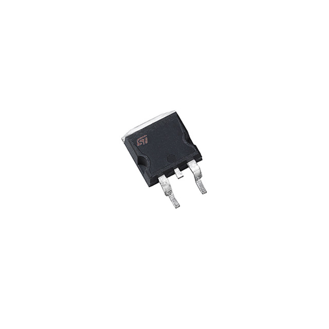
Using the latest high voltage technology based on a patented strip layout, STMicroelectronics has designed an advanced family of IGBTs, the PowerMESH™ IGBTs, with outstanding performances. The built in collector-gate zener exhibits a very precise active clamping while the gate-emitter zener supplies an ESD protection.
STGB7NB40LZ Maximum Ratings
Symbol
Parameter
Value
Unit
VCES
Collector-Emitter Voltage (VGS = 0)
CLAMPED
V
VECR
Emitter-Collector Voltage
20
V
VGE
Gate-Emitter Voltage
CLAMPED
V
IC
Collector Current (continuous) at Tc = 25 oC
14
A
RG
Minimum External Gate Resistor
500
W
PTOT
Total Dissipation at TC = 25°C
100
W
Derating Factor
0.66
W/°C
ECL
Single Pulse Collector to Emitter Avalanche Energy IC= 13 A ; Tj= 150°C (see fig.1-2)
130
mJ
EECAV
Reverse Avalanche Energy IC = 7 A ;f= 100 Hz ; Tc = 25°C
10
mJ
Tstg
Storage Temperature
55 to 150
oC
Tj
Operating Junction Temperature
STGB7NB40LZ Features
POLYSILICON GATE VOLTAGE DRIVEN LOW THRESHOLD VOLTAGE LOW ON-VOLTAGE DROP LOW GATE CHARGE HIGH CURRENT CAPABILITY HIGH VOLTAGE CLAMPING FEATURE