STG3680

Features: HIGH SPEED: D = 0.3ns (TYP.) at VCC = 3.0V D = 0.4ns (TYP.) at VCC = 2.3VULTRA LOW POWER DISSIPATION: C = 0.2A (MAX.) at TA = 85°CLOW ON RESISTANCE VIN = 0V: N-S1 = 0.5 (MAX. TA = 25°C) at VCC=2.7V N-S2 = 0.8 (MAX. TA = 25°C) at VCC=2.7VWIDE OPERATING VOLTAGE RANGE: C (OPR) = 1.65V to ...

product image

STG3680 Picture
SeekIC No. : 004507613 Detail

STG3680: Features: HIGH SPEED: D = 0.3ns (TYP.) at VCC = 3.0V D = 0.4ns (TYP.) at VCC = 2.3VULTRA LOW POWER DISSIPATION: C = 0.2A (MAX.) at TA = 85°CLOW ON RESISTANCE VIN = 0V: N-S1 = 0.5 (MAX. TA = 25°C) ...

floor Price/Ceiling Price

Part Number:
STG3680
Supply Ability:
5000

Price Break

  • Qty
  • 1~5000
  • Unit Price
  • Negotiable
  • Processing time
  • 15 Days
Total Cost: $ 0.00

SeekIC Buyer Protection PLUS - newly updated for 2013!

  • Escrow Protection.
  • Guaranteed refunds.
  • Secure payments.
  • Learn more >>

Month Sales

268 Transactions

Rating

evaluate  (4.8 stars)

Upload time: 2024/4/18

Payment Methods

All payment methods are secure and covered by SeekIC Buyer Protection PLUS.

Notice: When you place an order, your payment is made to SeekIC and not to your seller. SeekIC only pays the seller after confirming you have received your order. We will also never share your payment details with your seller.
Product Details

Description


Features:

 HIGH SPEED:
   D = 0.3ns (TYP.) at VCC = 3.0V
   D = 0.4ns (TYP.) at VCC = 2.3V
 ULTRA LOW POWER DISSIPATION:
   C = 0.2A (MAX.) at TA = 85°C
 LOW "ON" RESISTANCE VIN = 0V:
   N-S1 = 0.5 (MAX. TA = 25°C) at VCC=2.7V
   N-S2 = 0.8 (MAX. TA = 25°C) at VCC=2.7V
 WIDE OPERATING VOLTAGE RANGE:
   C (OPR) = 1.65V to 4.3V SINGLE SUPPLY
 4.3V TOLERANT AND 1.8V COMPATIBLE
   ESHOLD ON DIGITAL CONTROL INPUT t VCC = 2.3 to 3.0V
 LATCH-UP PERFORMANCE EXCEEDS 00mA (JESD 17)


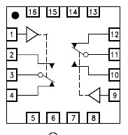
Pinout

  Connection Diagram


Specifications

Symbol
Parameter
Value
Unit
VCC
Supply Voltage
-0.5 to 4.6
V
VIDC
Input Voltage
-0.5 to VCC + 0.5
V
VIC
DC Control Input Voltage
-0.5 to 4.6
V
VO
DC Output Voltage
-0.5 to VCC + 0.5
V
IIKC
DC Input Diode Current on control pin (VIN< 0V)
− 50
mA
IIK
DC Input Diode Current (VIN< 0V)
± 50
mA
IOK
DC Output Diode Current
± 20
mA
IO
DC Output Current
± 300
mA
IOP
DC Output Current Peak (pulse at 1ms, 10% duty cycle)
± 500
mA
ICC or IGND
DC VCC or Ground Current
± 100
mA
PD
Power Dissipation at Ta=70°C (1)
1120
 
mW
 
Tstg
Storage Temperature
-65 to 150
°C
TL
Lead Temperature (10 sec)
300
°C


Description

The STG3680 is an high-speed CMOS DUAL NALOG S.P.D.T. (Single Pole Dual Throw) WITCH or DUAL 2:1 Multiplexer/Demultiplexer Switch fabricated in silicon gate C2MOS echnology. It is designed to operate from 1.65V to .3V, making this device ideal for portable pplications.

STG3680 offers very low ON-Resistance (<0.5 1S1 and S1 channels; <0.8 1S2 and 2S2 channels) at CC=2.7V. The nIN inputs are provided to control he switches. The switches nS1 are ON (they are onnected to common Ports Dn) when the nIN nput is held high and OFF (high impedance state xists between the two ports) when nIN is held ow; the switches nS2 are ON (they are connected o common Ports Dn) when the nIN input is held ow and OFF (high impedance state exists etween the two ports) when IN is held high. dditional key features are fast switching speed, reak Before Make Delay Time and Ultra Low ower Consumption. All inputs and outputs are quipped with protection circuits against static ischarge, giving them ESD immunity and ransient excess voltage. It's available in the ommercial temperature range in the QFN ackage.


Customers Who Bought This Item Also Bought

Margin,quality,low-cost products with low minimum orders. Secure your online payments with SeekIC Buyer Protection.
Cables, Wires - Management
Tapes, Adhesives
803
Prototyping Products
DE1
View more