
Circuit Diagram
Index
The output stage gain adjustment circuit (INA103)
Published:2014/5/26 20:47:00 Author:lynne | Keyword: The output stage gain adjustment circuit (INA103), INA103
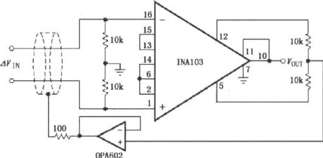
The output stage gain adjustment circuit (INA103) as shown:
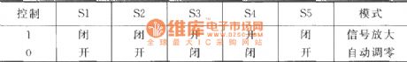
Gain selection as shown in the following table:
(View)
View full Circuit Diagram | Comments | Reading(9645)
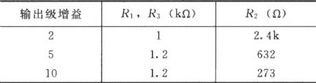
NC gain ± 1 amplifier (INA105)
Published:2014/5/26 20:45:00 Author:lynne | Keyword: NC gain ± 1 amplifier (INA105), INA105, DG188
NC gain ± 1 amplifier (INA105) circuit as shown:
(View)
View full Circuit Diagram | Comments | Reading(7057)
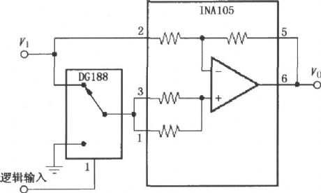
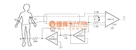
ECG recorder or biological signals preamplifier
Published:2014/5/26 20:42:00 Author:lynne | Keyword: ECG recorder or biological signals preamplifier, INA102
ECG recorder or biological signals preamplifier circuit as shown:
As shown ECG recorder or biological signals preamplifier. Human bio-electricity is a weak signal, it should be noted each electrode contact resistance and the body should be as small as possible to reduce measurement error. (View)
View full Circuit Diagram | Comments | Reading(8947)
Auto-zero instrumentation amplifier (INA102)
Published:2014/5/26 20:37:00 Author:lynne | Keyword: Auto-zero instrumentation amplifier (INA102), INA102, DG5043CJ, OPA111, OPA121, DG5040CJ
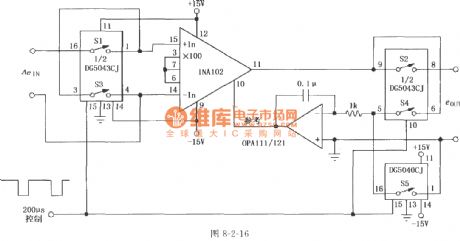
Auto-zero instrumentation amplifier (INA102) circuit as shown:
As shown for the auto-zero instrumentation amplifier. DG5043CJ and DG5040CJ as analog switches, with 200μs control signal controls the analog switch is closed or open. When 200μs control signal is high open days 1 when closed, low level 0 when the switch is turned off, thereby amplifying the signal control circuit is in a state or in auto-zero state of their work, see the following table.
(View)
View full Circuit Diagram | Comments | Reading(7958)
Externally adjustable CMR (common mode rejection ratio) circuit (INA103)
Published:2014/5/26 20:38:00 Author:lynne | Keyword: Externally adjustable CMR (common mode rejection ratio) circuit (INA103), INA103
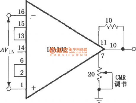
Externally adjustable CMR (common mode rejection ratio) circuit (INA103) shown as follow:
(View)
View full Circuit Diagram | Comments | Reading(6507)
The right leg drive ECG amplifier (INA114)
Published:2014/5/22 21:09:00 Author:lynne | Keyword: The right leg drive ECG amplifier (INA114), INA114
The right leg drive ECG amplifier (INA114) circuit as shown:
As shown in the right leg drive ECG amplifier. Human bioelectricity as the weak current signal, in the right leg drive ECG ECG amplifier using shielding wire transfer human weak current signal, the 1/2 opa2604 voltage follower, as the anti-interference measures shielded wire drive; Another 1/2 opa2604 to form the inverting amplifier gain for 39, drive to the right leg. Through both signal shield cable transmission input INA114, after INA114 amplifier output, G = 10. (View)
View full Circuit Diagram | Comments | Reading(9915)
Gain for 1/2 precision amplifying circuit (INA105)
Published:2014/5/22 21:06:00 Author:lynne | Keyword: Gain for 1/2 precision amplifying circuit (INA105), INA105
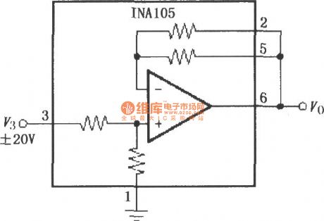
Gain for 1/2 precision amplifying circuit (INA105) as shown:
As shown for gain = 1/2 precision amplifying circuit. The circuit is connected the two foot to 5 foot ably, internal two Ω 25 k resistor in parallel, constitute a gain for 1/2 in-phase amplifier, the output voltage Vo = 1/2 v3, gain error = 0.01% (maximum). (View)
View full Circuit Diagram | Comments | Reading(6741)
Gain 11 of precision buffer circuit(INA106)
Published:2014/5/22 21:01:00 Author:lynne | Keyword: Gain 11 of precision buffer circuit(INA106), INA106
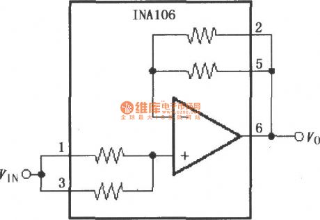
Gain 11 of precision buffer circuit(INA106) as shown:
(View)
View full Circuit Diagram | Comments | Reading(6503)
Gain 2 of precision amplifier circuit (INA105)
Published:2014/5/22 20:58:00 Author:lynne | Keyword: Gain 2 of precision amplifier circuit (INA105), INA105
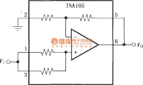
Gain 2 of precision amplifier circuit (INA105) as shown:
As shown for precision amplifier circuit gain = 2. The circuit will be 1 to 3 feet feet, ably internal two Ω 25 k resistor in parallel, constitute a in-phase amplifier. The output voltage Vo = 2 v1, gain error = 0.01% (maximum), gain drift = 2 x 10⁻⁶ /℃. (View)
View full Circuit Diagram | Comments | Reading(6676)
OPA1013 and INA117 constitute of the current detection circuit of the input buffer
Published:2014/5/22 20:54:00 Author:lynne | Keyword: OPA1013 and INA117 constitute of the current detection circuit of the input buffer, OPA1013, INA117
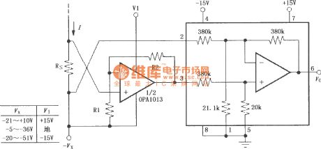
OPA1013 and INA117 constitute of the current detection circuit of the input buffer as shown:
As shown by the input buffer OPA1013 constitute a current detection circuit. In the INA117 inputs plus a buffer amplifier gain errors can make zero or common-mode rejection ratio decreased. OPA1013 can constitute a voltage follower (short R2, omit R1); may also constitute a gain inverting amplifier with a gain can be improved INA117 forward channel SNR and CMR, while allowing the sample may have a lower resistance voltage drop. Select OPA1013 op amp as a buffer allows the input and output voltage swing close to the negative supply. V0 = IRs (1 + R2/R1).
(View)
View full Circuit Diagram | Comments | Reading(7041)
The OPA340 composed of INA321/322 output buffer circuit
Published:2014/5/21 21:07:00 Author:lynne | Keyword: The OPA340 composed of INA321/322 output buffer circuit, OPA340, INA321, INA322
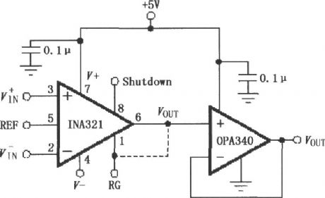
The OPA340 composed of INA321/322 output buffer circuit as shown:
As shown configured by OPA340 of INA321/322output buffer circuit. INA321/322 optimum load impedance of 10kΩ or greater. When the load impedance is reduced, the output current will increase. OPA340 op amp with a voltage follower as constituting an output buffer circuit for increasing INA321/322 output drive capability. OPA340 output voltage swing is less than the maximum supply voltage 50mV, capable of driving up to 600Ω load. (View)
View full Circuit Diagram | Comments | Reading(6565)
The OPA340 composed of INA331/332 output buffer circuit
Published:2014/5/21 20:59:00 Author:lynne | Keyword: The OPA340 composed of INA331/332 output buffer circuit, INA331, OPA340
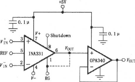
The OPA340 composed of INA331/332 output buffer circuit as shown:
As shown by INA331/332 OPA340 output buffer circuit configured. INA331/332 optimum load impedance of 10kΩ or greater. When the load impedance is reduced, the output current will increase, shown with OPA340 op amp voltage follower as constituting an output buffer circuit to increase INA331/332 output drive capability, OPA340 maximum output voltage swing below the supply voltage 50mV , capable of driving up to 600Ω load.
(View)
View full Circuit Diagram | Comments | Reading(6558)
Constituted by the OPA602 feedback AC coupling circuit (INA117)
Published:2014/5/21 20:37:00 Author:lynne | Keyword: Constituted by the OPA602 feedback AC coupling circuit (INA117), INA117, OPA602
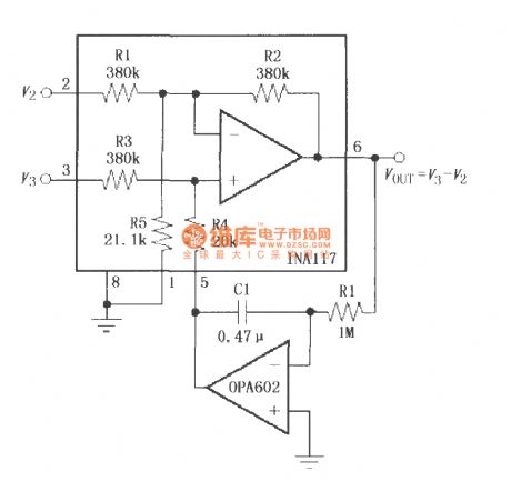
Constituted by the OPA602 feedback AC coupling circuit (INA117) shown as follow:
(View)
View full Circuit Diagram | Comments | Reading(6313)
Constituted by the INA118 differential voltage - current converter
Published:2014/5/21 20:31:00 Author:lynne | Keyword: Constituted by the INA118 differential voltage - current converter, INA118
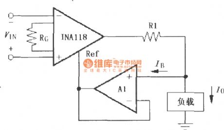
Constituted by the INA118 differential voltage - current converter circuit as shown:
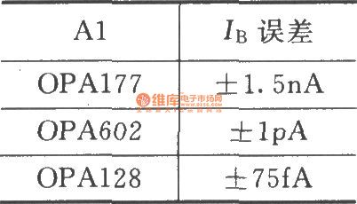
As shown by INA118 constitute differential voltage - current converter. INA118 current source constituted by the output of R1 and A1, due to high input impedance of the operational amplifier, the bias current is extremely small, and the output current to the load is negligible compared to, so the output current Io can be considered constant, and only the input voltage and R1 concerned that Io = (VIN/R1) × G. A1 Selection and IB error below. >The current source output current Io within a certain range regardless of the load, the input voltage and depends only on the resistors R1, when R1 is fixed, the output current and the input voltage VIN related only to complete the differential voltage - current conversion.
(View)
View full Circuit Diagram | Comments | Reading(7864)
Constituted by the INA102 and PGA102 of programmable instrumentation amplifier
Published:2014/5/21 20:36:00 Author:lynne | Keyword: Constituted by the INA102 and PGA102 of programmable instrumentation amplifier, INA102, PGA102
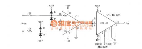
Constituted by the INA102 and PGA102 of programmable instrumentation amplifier circuit as shown:
As shown by INA102 and PGA102 a programmable instrumentation amplifier. This circuit uses the INA102 and PGA102 cascade, INA102 gain of 1, while the PGA102 gain selectable. The circuit is characterized by the use INA102 input impedance matching and signal sources, while using a microprocessor using PGA102 programmable gain characteristics of its choice. INA102 inputs, respectively, with four diode limiter, input overvoltage to prevent damage to the internal circuitry. Diode leakage current must be selected pipe, otherwise leakage current will weaken the signal attenuation that can not amplify weak signals. D for input protection diode, use FDH300 (low leakage current). (View)
View full Circuit Diagram | Comments | Reading(6312)
Constituted by the INA118 AC-coupled instrumentation amplifier
Published:2014/5/20 20:58:00 Author:lynne | Keyword: Constituted by the INA118 AC-coupled instrumentation amplifier, INA118, OPA602
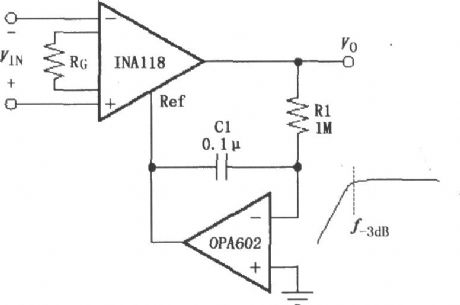
Constituted by the INA118 AC-coupled instrumentation amplifier circuit as shown:
As shown by the AC-coupled constitute INA118 instrumentation amplifier. OPA602 constitute a feedback circuit with AC characteristics, f-3db = 1/2πR1C1 = 1.59Hz. The signal is fed to the Ref INA118 end (5 feet), which formed the AC coupling circuit. (View)
View full Circuit Diagram | Comments | Reading(7368)
Constituted by the INA118 single supply bridge amplifier
Published:2014/5/20 20:59:00 Author:lynne | Keyword: Constituted by the INA118 single supply bridge amplifier, INA118
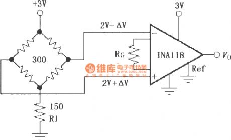
Constituted by the INA118 single supply bridge amplifier circuit as shown:
(View)
View full Circuit Diagram | Comments | Reading(7280)
Constituted by the INA118 cold junction compensation thermocouple amplifier
Published:2014/5/20 20:57:00 Author:lynne | Keyword: Constituted by the INA118 cold junction compensation thermocouple amplifier, INA118, REF102, PT100
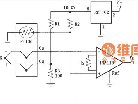
Constituted by the INA118 cold junction compensation thermocouple amplifier circuit shown as follow:
As shown by INA118 constituted cold junction compensation thermocouple amplifier. Using REF102 precision reference voltage source (10V) power supply for the thermocouple.
(View)
View full Circuit Diagram | Comments | Reading(7871)
Constituted by the INA122, single-supply current shunt measurement circuit
Published:2014/5/20 20:55:00 Author:lynne | Keyword: Constituted by the INA122, single-supply current shunt measurement circuit, INA122, REF200
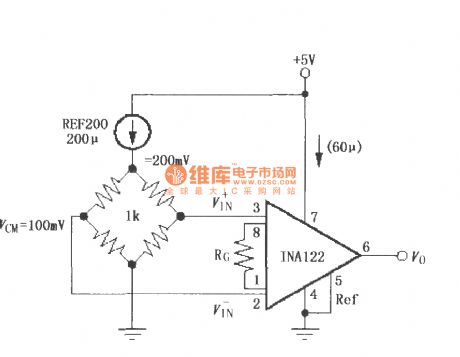
Constituted by the INA122, single-supply current shunt measurement circuit as shown:
(View)
View full Circuit Diagram | Comments | Reading(7393)
Single power resistor bridge constructed by the INA125 amplifier
Published:2014/5/20 20:54:00 Author:lynne | Keyword: Single power resistor bridge constructed by the INA125 amplifier, INA125
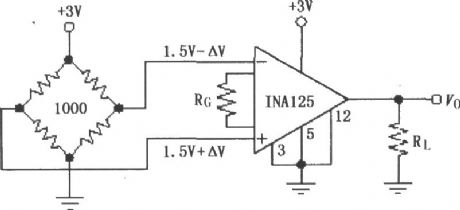
Single power resistor bridge constructed by the INA125 amplifier circuit as shown:
(View)
View full Circuit Diagram | Comments | Reading(8467)
| Pages:1/2234 1234567891011121314151617181920Under 20 |
Circuit Categories
power supply circuit
Amplifier Circuit
Basic Circuit
LED and Light Circuit
Sensor Circuit
Signal Processing
Electrical Equipment Circuit
Control Circuit
Remote Control Circuit
A/D-D/A Converter Circuit
Audio Circuit
Measuring and Test Circuit
Communication Circuit
Computer-Related Circuit
555 Circuit
Automotive Circuit
Repairing Circuit