
Circuit Diagram
Index 2
Composed of INA126 differential voltage to current conversion circuit
Published:2014/5/19 20:48:00 Author:lynne | Keyword: Composed of INA126 differential voltage to current conversion circuit, INA126
Composed of INA126 differential voltage to current conversion circuit as shown:
As shown by INA126 differential voltage to current conversion circuit. INA126 output by R1 and A1 constitute a current source, because of high input impedance, bias current remote operational amplifiers, compared with the output to the load current can be neglected, so the output current Io can be regarded as a constant, only related to the input voltage and R1. Io = (VIN/R1) x G. See table A1 selection and IB error. Figure in the dotted line connected to INA2126 encapsulation (16 feet) Sensn end connected to the Vo output end, used to detect the output voltage changes. Current source output current Io has nothing to do with the load within a certain scope, only depends on the input voltage and resistor R1, when R1 is fixed, the output current is only related to the input voltage VIN, can complete differential voltage - current transformation.
(View)
View full Circuit Diagram | Comments | Reading(2754)
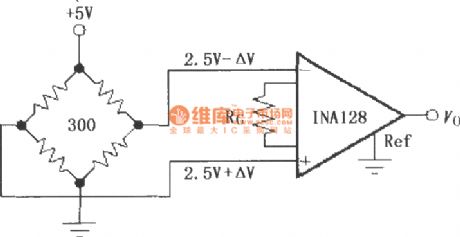
Constituted by the INA128 AC-coupled instrumentation amplifier
Published:2014/5/19 20:43:00 Author:lynne | Keyword: Constituted by the INA128 AC-coupled instrumentation amplifier, INA128, OPA130
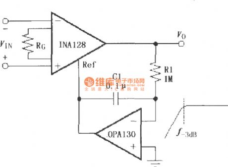
Constituted by the INA128 AC-coupled instrumentation amplifier circuit as shown:
As shown by instrumentation amplifier INA128 constitute communication coupling. OPA130 constitute the communication characteristics of feedback circuit (f - 3 db = 1/2 PI R1C1), the signal feedback to the Ref INA128 (5 feet), the coupled circuit of communication. (View)
View full Circuit Diagram | Comments | Reading(2523)
Composed of INA128 differential voltage to current conversion circuit
Published:2014/5/19 20:44:00 Author:lynne | Keyword: Composed of INA128 differential voltage to current conversion circuit, INA128
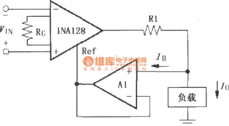
Composed of INA128 differential voltage to current conversion circuit shown as follow:
As shown by INA128 differential voltage to current conversion circuit. INA128 output by the R1 and A1 constitute a current source, output current Io is considered to be a constant, only related to the input voltage and R1, Io = (VIN/R1) x G. (View)
View full Circuit Diagram | Comments | Reading(1837)
Constituted by the INA131 differential voltage - current conversion circuit
Published:2014/5/19 20:35:00 Author:lynne | Keyword: Constituted by the INA131 differential voltage - current conversion circuit, INA131
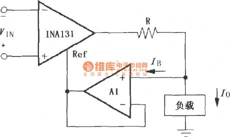
Constituted by the INA131 differential voltage - current conversion circuit as shown:
s shown constituted by the differential voltage INA131 - current conversion circuit. INA131 output constituted by the current sources A1 and R, because high input impedance operational amplifier, the bias current is extremely small, and the output current to the load is negligible compared to, so the output current Io can be considered constant, and only the input voltage and R about, Io = 100VIN / R (gain = 100). A1 Selection and IB error below. (View)
View full Circuit Diagram | Comments | Reading(1485)
Constituted by INA128, a cold junction compensation thermocouple amplifier
Published:2014/5/19 20:41:00 Author:lynne | Keyword: Constituted by INA128, a cold junction compensation thermocouple amplifier, INA128, REF102
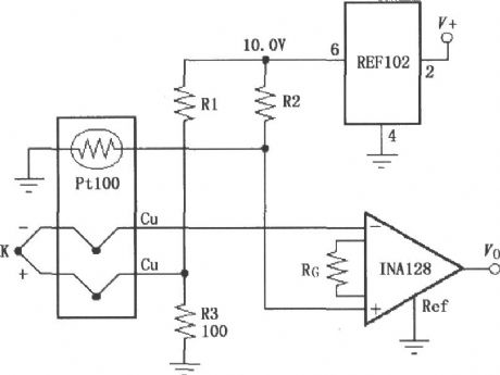
Constituted by INA128, a cold junction compensation thermocouple amplifier circuit as shown:
As shown INA128 constituted by cold junction compensation thermocouple amplifier. Using REF102 precision reference voltage source (10.0V) thermocouple power. Selection of the thermocouple and the resistance R1, R2 shown in the table match. (View)
View full Circuit Diagram | Comments | Reading(3396)
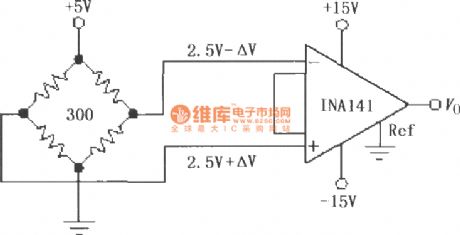
Constituted by INA131, the resistor bridge amplifier
Published:2014/5/18 20:36:00 Author:lynne | Keyword: Constituted by INA131, the resistor bridge amplifier, INA131
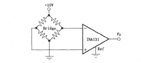
Constituted by INA131, the resistor bridge amplifier circuit as shown:
(View)
View full Circuit Diagram | Comments | Reading(1680)
Constituted by the INA131 AC-coupled instrumentation amplifier
Published:2014/5/18 20:34:00 Author:lynne | Keyword: Constituted by the INA131 AC-coupled instrumentation amplifier, INA131, OPA602
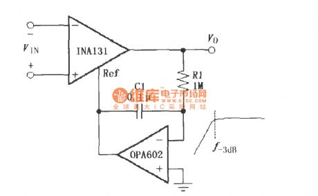
Constituted by the INA131 AC-coupled instrumentation amplifier circuit as shown:
As shown by INA131 instrumentation amplifier composed of AC-coupled. OPA602 constitute a feedback circuit with AC characteristics (f-3db = 1/2πR1C1), the signal is fed to the INA131's Ref side (5 feet), which formed the AC coupling circuit. (View)
View full Circuit Diagram | Comments | Reading(1539)
INA131 configuration of the shield drive circuit
Published:2014/5/18 20:27:00 Author:lynne | Keyword: INA131 configuration of the shield drive circuit, INA131, OPA602
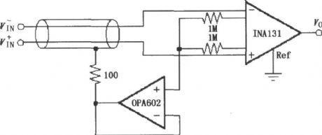
INA131 configuration of the shield drive circuit as shown:
As shown by the shield drive circuit configured INA131. Evidenced by the interference theory and practice in the cable shield weak signal transmission with a certain potential, will greatly reduce the interference between the shield and the core introduced by the distributed capacitance coupling. The circuit is based on this consideration, with the OPA602 as constituting a voltage follower drive shield generator, the input signal from the internal op-amp instrumentation amplifier, OPA602 output to shield that shields the potential to be elevated to the internal amp potential of the output amplifier, so that the interference on the cable is significantly reduced. The presence of common mode voltage shielded line is driven, the resistance of the common mode gain of about 0.1%.
(View)
View full Circuit Diagram | Comments | Reading(2874)
Constituted by the INA141 AC-coupled instrumentation amplifier
Published:2014/5/18 20:07:00 Author:lynne | Keyword: Constituted by the INA141 AC-coupled instrumentation amplifier, INA141, OPA602
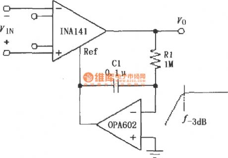
Constituted by the INA141 AC-coupled instrumentation amplifier circuit as shown:
As shown by the AC-coupled constitute INA141 instrumentation amplifier. OPA602 constitute a feedback circuit with AC characteristics (f-3db = 1/2πR1C1), the signal is fed to the INA141's Ref side (5 feet), which formed the AC coupling circuit. (View)
View full Circuit Diagram | Comments | Reading(1559)
Constituted by INA141 resistor bridge amplifier
Published:2014/5/18 20:25:00 Author:lynne | Keyword: Constituted by INA141 resistor bridge amplifier, INA141
Constituted by INA141 resistor bridge amplifier circuit shown as follow:
(View)
View full Circuit Diagram | Comments | Reading(1562)
Thermocouple constituted by the INA141 amplifier with cold junction compensation circuit
Published:2014/5/15 22:03:00 Author:lynne | Keyword: Thermocouple constituted by the INA141 amplifier with cold junction compensation circuit, INA141, Pt100, REF102
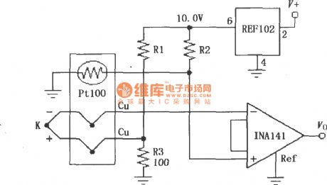
Thermocouple constituted by the INA141 amplifier with cold junction compensation circuit as shown:
As shown by INA141 constitute thermocouple with cold junction compensation amplifier circuit. REF102 precision reference power using thermocouples provide operating voltage, the voltage generated by the thermocouple INA114 preamp output. K-type thermocouple. (View)
View full Circuit Diagram | Comments | Reading(3120)
Input current protection circuit constituted by the INA155/156
Published:2014/5/15 21:41:00 Author:lynne | Keyword: Input current protection circuit constituted by the INA155/156, INA155
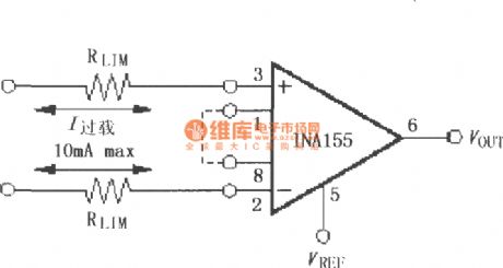
Input current protection circuit constituted by the INA155/156 circuit as shown:
As shown by INA155/156 constitute input current protection circuit. INA155 inputs have internal electrostatic discharge (ESD) protection diodes, when the input voltage exceeds the supply voltage of 500mV, protection diodes will turn on, then RLIM will limit the input current (maximum 10mA), play a role in the protection circuit. Many of the input signal itself is limited streaming capabilities, which limit the flow resistance RLIM can not.
(View)
View full Circuit Diagram | Comments | Reading(2110)
Configured INA155/156 directly driven by a capacitive input high speed A / D converter
Published:2014/5/15 21:33:00 Author:lynne | Keyword: Configured INA155/156 directly driven by a capacitive input high speed A / D converter, INA155, INA156, ADS7818, ADS7834
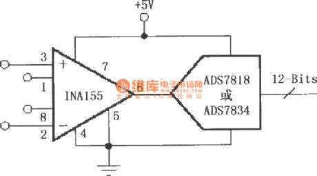
Configured INA155/156 directly driven by a capacitive input high speed A / D converter circuit as shown:
A capacitive high-speed direct drive input configured as shown in FIG INA155/156 by the A / D converter in Figure G = 10. After INA155 input voltage amplification to 12 high-speed low-power sampling A / D converter ADS7818 or ADS7834. ADS7818 or ADS7834 inputs for the internal capacitor array (CDAC), is the capacitive input, analog signal conversion A / D converter input is 12-bit digital signal output, fsample = 500kHz. (View)
View full Circuit Diagram | Comments | Reading(2290)
Input current protection circuit constituted by the INA321/322
Published:2014/5/15 21:29:00 Author:lynne | Keyword: Input current protection circuit constituted by the INA321/322, INA321, INA322
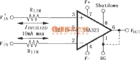
Input current protection circuit constituted by the INA321/322 circuit as shown:
As shown by INA321/322 constitute input current protection circuit. INA321/322 inputs have internal electrostatic discharge (ESD) protection diodes, when the input voltage exceeds the supply voltage of 500mV, protection diodes will turn on, then RLIM will limit the input current (maximum 10mA), play a role in the protection circuit. Many of the input signal itself is limited streaming capabilities, which limit the flow resistance RLIM can not.
(View)
View full Circuit Diagram | Comments | Reading(2179)
INA321/322 constituted by a direct drive capacitive input A / D converter
Published:2014/5/15 20:35:00 Author:lynne | Keyword: INA321/322 constituted by a direct drive capacitive input A / D converter, INA321, ADS7818, ADS7822
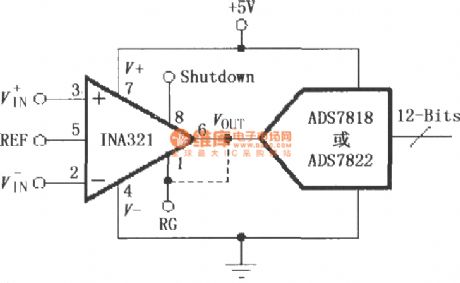
INA321/322 constituted by a direct drive capacitive input A / D converter circuit as shown:
As shown directly driving a capacitive input constituted by INA321/322 A / D converter. Since INA321/322 output is a low, so you can work at high frequencies directly drive capacitive loads. After INA321/322 amplified input voltage output, directly to the 12 high-speed low-power sampling A / D converter ADS7818 or ADS7822. ADS7818 or ADS7822 internal input terminal of the capacitor array (CDAC) digital-analog conversion, is a capacitive input, converts the analog signal A / D converter 12 converts the input digital signal output. (View)
View full Circuit Diagram | Comments | Reading(2121)
Composed of INA331/332 resistance bridge sensor amplifier
Published:2014/5/14 21:15:00 Author:lynne | Keyword: Composed of INA331/332 resistance bridge sensor amplifier, INA331, INA332
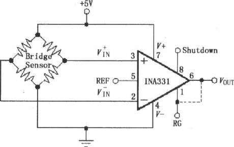
Composed of INA331/332 resistance bridge sensor amplifier circuit as shown:
(View)
View full Circuit Diagram | Comments | Reading(1774)
Composed of INA331/332 direct drive capacitive input A/D converter
Published:2014/5/14 21:14:00 Author:lynne | Keyword: Composed of INA331/332 direct drive capacitive input A/D converter, INA331, ADS7818, ADS7822
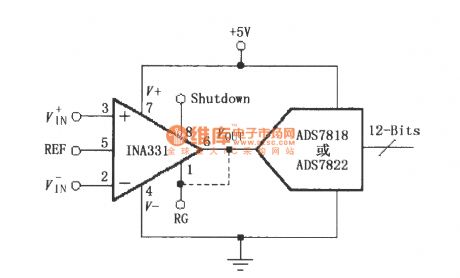
Composed of INA331/332 direct drive capacitive input A/D converter circuit as shown:
As shown by INA331/332 consisting of direct drive capacitive input A/D converter. Because INA331/332 output for low resistance, when working in high frequency can be directly driving capacitive loads. The input voltage through the INA331 amplifier output, directly to 12 low-power high-speed sampling A/D converter ADS7818 or ADS7822. ADS7818 or ADS7822 internal input capacitance array (CDAC) D/A conversion, namely for the capacitive input, A/D converter input analog signal is converted to 12 digital signal output. (View)
View full Circuit Diagram | Comments | Reading(1989)
Composed of load current high-end INA337 shunt measurement circuit
Published:2014/5/14 21:12:00 Author:lynne | Keyword: Composed of load current high-end INA337 shunt measurement circuit, INA337
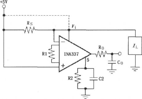
Composed of load current high-end INA337 shunt measurement circuit as shown:
As shown by INA337 high-end shunt measurement circuit composed of load current. The circuit adopts the sampling resistor Rs series between the source and load, load current IL through Rs will produce a voltage drop, the voltage drop reflects the changes in load current. Will be as input voltage, the voltage drop across the Rs after INA337 amplifier output. Should be paid attention to when selecting Rs in Rs on the formation of the Rail voltage drop cannot exceed supply voltage (maximum) 100 mv. R0, C0, output filter network, can filter out noise circuit output. (View)
View full Circuit Diagram | Comments | Reading(2103)
Composed of INA337 output reference potential to VREF / 2 circuit
Published:2014/5/14 21:08:00 Author:lynne | Keyword: Composed of INA337 output reference potential to VREF / 2 circuit, INA337
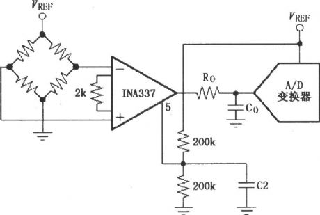
Composed of INA337 output reference potential to VREF / 2 circuit shown as follow:
As shown by INA337 constitute the output of the reference potential for VREF / 2 circuits. When unbalanced bridge, the bridge output voltage by the output after INA337 magnified 100 times, after filter composed of Ro and Co filter out noise, and sent to the A/D converter converts analog signals to digital signals. In 5 feet with two 200 k Ω INA337 resistance partial pressure, VREF / 2 potential, potential to VREF / 2 to 5 feet. Output voltage is 5 feet for reference potential, so the output potential becomes relatively to VREF / 2 for reference. G = 2 (200 k Ω ∥ Ω) 200 k / 2 k Ω = 100. (View)
View full Circuit Diagram | Comments | Reading(2389)
Composed of INAl28 resistance bridge amplifier
Published:2014/5/14 21:05:00 Author:lynne | Keyword: Composed of INAl28 resistance bridge amplifier, INA128
Composed of INAl28 resistance bridge amplifier circuit as shown:
(View)
View full Circuit Diagram | Comments | Reading(1591)
| Pages:2/2234 1234567891011121314151617181920Under 20 |
Circuit Categories
power supply circuit
Amplifier Circuit
Basic Circuit
LED and Light Circuit
Sensor Circuit
Signal Processing
Electrical Equipment Circuit
Control Circuit
Remote Control Circuit
A/D-D/A Converter Circuit
Audio Circuit
Measuring and Test Circuit
Communication Circuit
Computer-Related Circuit
555 Circuit
Automotive Circuit
Repairing Circuit