
Circuit Diagram
Index 11
10-pin low-power digital temperature sensor circuit diagram
Published:2014/3/26 21:45:00 Author:lynne | Keyword: 10-pin low-power digital temperature sensor circuit diagram
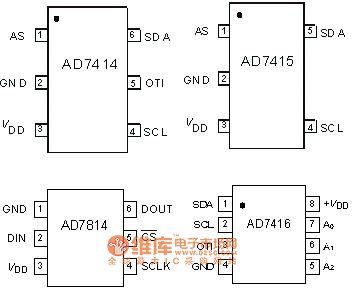
AD7414, AD7415, AD7416, AD7814 and other four models, they work the same pinout as shown:
(View)
View full Circuit Diagram | Comments | Reading(3107)
Fan controller circuit
Published:2014/3/26 21:44:00 Author:lynne | Keyword: Fan controller circuit
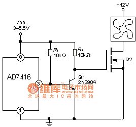
Fan controller circuit shown as follow:
(View)
View full Circuit Diagram | Comments | Reading(3198)
Eight AD7416 parallel circuit diagram
Published:2014/3/26 21:43:00 Author:lynne | Keyword: Eight AD7416 parallel circuit diagram, AD7416
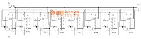
D7416 serial address low 3 can be set by the user, allowing a choice from 1001000 to 1001111 of eight addresses. 8 illustrates the AD7416 has received a serial bus system, their OTI output line to form a common interrupt request lines.
(View)
View full Circuit Diagram | Comments | Reading(1528)
Hardware schematic circuit
Published:2014/3/26 21:41:00 Author:lynne | Keyword: Hardware schematic circuit
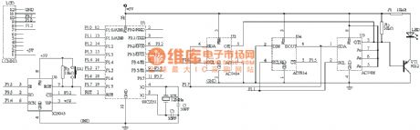
Hardware schematic is shown in Figure. This is an evaluation circuit, which can install three digital temperature sensor: AD7414, AD7416, AD7814, the software displays each device in turn measured ambient temperature and OTI analog outputs with LED indication. Some explanations are now as follows:
(1) address of each device is different, and SDA, DOUT leads can be connected directly; AD7414, OTI output line (active low), now overrun alarm indication for the AD7416. (2) due to the inertia of the temperature coefficient of the larger, can be a simple and effective method of moving average, median method, low-pass filtering method for software filtering. In practical applications, the side of the sample side, the average of the average value as the temperature samples. Sampling frequency of 8 to 16 times can be. (3) The system uses LCM103 LCD module for temperature display, X25045 for power-on reset and watchdog with. (View)
View full Circuit Diagram | Comments | Reading(1646)
MPX2100 pressure sensor and its application circuit diagram Ⅰ
Published:2014/3/26 21:37:00 Author:lynne | Keyword: MPX2100 pressure sensor and its application circuit diagram Ⅰ, MPX2100
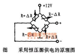
Works MPX2100 has four pins, between an output pin to ground, 3 feet plus working pressure, 2 feet and 4 feet and differential mode voltage signal proportional to the pressure. MPX2100 is a piezoresistive pressure sensor, made on a silicon substrate diffusion process four equal resistor strain elements constituting the Wheatstone bridge. Bridge has a constant voltage source and a constant current source power supply two power supply. Constant voltage source power supply schematic diagram shown in Fig.
When the pressure sensor is subjected to pressure, the resistance value of a bridge arm to increase ΔR, the other arm of the resistance value is reduced ΔR, the change of resistance ΔR proportional to the pressure, i.e. ΔR = KP, the bridge output voltage Uo = E (ΔR / R) = (EK / R) P, i.e., the bridge output voltage proportional to the pressure P.
(View)
View full Circuit Diagram | Comments | Reading(3178)
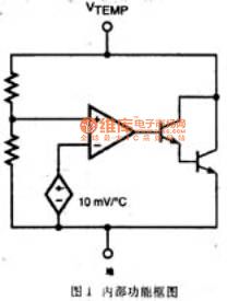
Four packages of AS300 circuit board
Published:2014/3/25 21:38:00 Author:lynne | Keyword: Four packages of AS300 circuit board, AS300
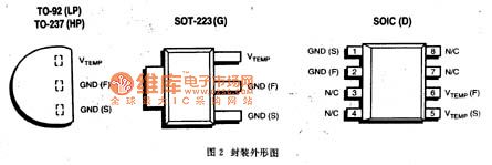
AS300 four packages shown (top view), each pin functions:
GND (S) selectable detection feet ground, and the substrate GND GND (F) is not connected. GND (F): signal ground and the circuit substrate grounding pin. VTEMP (F): output pin. The pin voltage is proportional to temperature. When 27 ℃, VTEMP = 3V, VTEMP with increasing temperature at a rate of 10mV / ℃ increases. VTEMP (S): selectable sensor VTEMP the output, use only on 8LSOIC package. (View)
View full Circuit Diagram | Comments | Reading(1401)
Digital pressure gauge based on MPX2100 circuit diagram
Published:2014/3/25 21:34:00 Author:lynne | Keyword: Digital pressure gauge based on MPX2100 circuit diagram, MPX2100
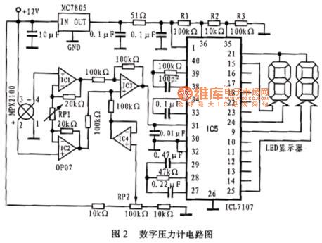
Digital pressure gauge based MPX2100 Digital pressure gauge MPX2100 configured as shown. MPX2100 operating voltage of 12V, the pressure between the sensor signal output 4 feet and 2 feet to IC1, IC2 amplification, amplifier gain is 1 +40 / RP1, IC1, IC2 connected to non-inverting input impedance state, the instrument can be obtained required high input impedance amplifier; IC3 is a unity gain differential amplifier, which can achieve high CMRR, IC4 and RP2 voltage divider circuit zeroing circuitry, RP1 used to adjust the gain of the amplifier circuit to complete the full digital display of pressure calibration range. IC3 output voltage to the A / D converter analog input voltage terminal IC5 (31 feet), the digital conversion by IC5 to drive LED display size of the pressure.
(View)
View full Circuit Diagram | Comments | Reading(3316)
Voltage frequency conversion composed MPX2100 circuit diagram
Published:2014/3/25 21:33:00 Author:lynne | Keyword: Voltage frequency conversion composed MPX2100 circuit diagram, MPX2100
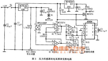
Voltage frequency conversion power
Figure is constituted by the voltage frequency conversion circuit MPX2100 . The circuit consists of a voltage amplification and frequency conversion of two parts, by a 4 op amp and a few resistors amplifier circuit , which has differential mode gain and high common-mode rejection ratio , and high input impedance, you can adjust the bias circuit. Differential amplifier circuit is mainly done by A1, A2 op amp feedback circuit is used to prevent the inflow of sensor negative side . At zero pressure, the difference between the voltage of the sensor between 2 feet and 4 feet to zero . If 2 feet and 4 feet each common-mode voltage 4V ( half the supply voltage sensor ), the A1 is a pin voltage is also 4V, so that the voltage through the A3 and A4 road to its output voltage is zero pressure . Zero pressure offset introduced by the output of R4 and R12, R12 can be set to adjust the bias voltage. By R7 choose from 13 feet to see past impedance , typically 1kΩ. Amplifier gain AV = R5 [1 + (R11/R10)] / R6 = 125. Select a gain of 125 allows the sensor full scale output swing amplified when 32mV to 4V swing .A3 output terminal voltage of 0.5 ~ 4.5V after by V / F conversion to the output frequency 1 ~ 10kHz . A3 8 feet and AD654V / F converter is connected . Its full- scale output frequency is determined by R3, R13 and C3, and can be calculated according to the following formula :Fout ( Full Scale ) = Vin / [10 (R3 + R15) C3] (View)
View full Circuit Diagram | Comments | Reading(2724)
External buffer remote temperature measurement circuit diagram
Published:2014/3/25 21:31:00 Author:lynne | Keyword: External buffer remote temperature measurement circuit diagram,
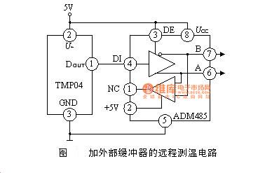
After the microcontroller coupled TMP03/04 easily microcomputer were measured in a counter t1, t2, then the software calculates the temperature. Because TMP03/04 is time ratio (t1/t2) to measure the temperature, so the computer does not require a very precise frequency counting, but counting frequency should be high enough.
(View)
View full Circuit Diagram | Comments | Reading(2028)
AS300 both ends of the integrated temperature sensor circuit diagram
Published:2014/3/25 21:29:00 Author:lynne | Keyword: AS300 both ends of the integrated temperature sensor circuit diagram, AS300
AS300 both ends of the integrated temperature sensor, is essentially a high-precision shunt regulator. Internal block diagram as shown. The output voltage proportional to the temperature sensor 27 ℃ when the output voltage is 3V, then the ratio of linear 10mV / ℃ increases. The sensor has a high accuracy, low output impedance, good linearity, etc., is an ideal device temperature detection.
AS300 There are four packages: TO-92, TO-237, SOT-223 packaged devices require larger heatsink. Using the TO-237 package, the device can be composed of ideal air temperature sensor. SOT-223 package uses the device is a hybrid substrate and the main MCM substrate temperature sensing devices. Such as requiring little installation space, high accuracy, the use of 8LSOIC package AS300 more suitable.
(View)
View full Circuit Diagram | Comments | Reading(1946)
Doppler effect sensor RD9481 application circuit diagram
Published:2014/3/24 21:32:00 Author:lynne | Keyword: Doppler effect sensor RD9481 application circuit diagram, RD9481
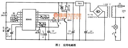
>Application Circuit
>RD9481R typical application circuit shown in Figure 2, the circuit is auto-sensing circuit lights, daytime lights are not bright, not bright at night when no one around, lights turn on automatically when someone walking.
After mains 220V transformer transformer, rectifier by (V1 ~ V4), the filter capacitor C4 and the voltage regulator circuit 7812 to get the DC supply voltage. RG photosensitive resistor R1 connected in series with the power supply voltage, the voltage divider circuit composed. During the day light shines onto the photosensitive resistor RG, RG showed low resistance, RD9481 5 feet low, blocking the trigger signal, the circuit does not work; night RG was high resistance, RD9481 5 feet high, so that the circuit to work . S is working mode selection switch, S is closed as a duplicate trigger work, S open to non-repeatable trigger work. Adjusting RP1, the sensitivity of the circuit can be adjusted to change the detection range can be adjusted to change the output high RP2 delay time adjustment block RP3 can change the timer has expired. (View)
View full Circuit Diagram | Comments | Reading(2966)
Transistor bistable trigger circuit diagram
Published:2014/3/24 21:29:00 Author:lynne | Keyword: Transistor bistable trigger circuit diagram
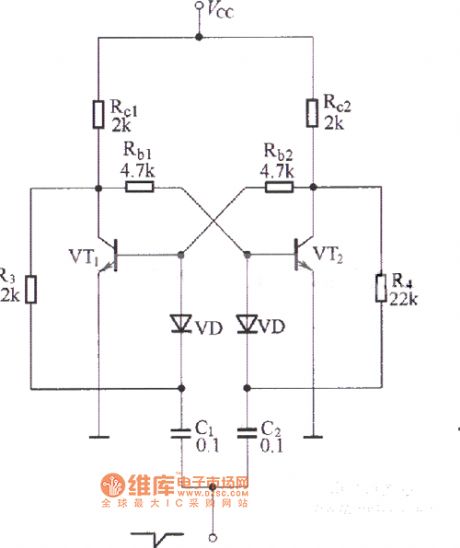
Transistor bistable trigger circuit diagram as shown:
(View)
View full Circuit Diagram | Comments | Reading(2730)
By an order bandpass filter of an operational amplifier circuit diagram
Published:2014/3/24 21:27:00 Author:lynne | Keyword: By an order bandpass filter of an operational amplifier circuit diagram
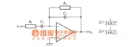
By an order bandpass filter of an operational amplifier circuit diagram as shown:
(View)
View full Circuit Diagram | Comments | Reading(1666)
Multiple feedback type second-order bypass filter circuit diagram
Published:2014/3/24 21:26:00 Author:lynne | Keyword: Multiple feedback type second-order bypass filter circuit diagram
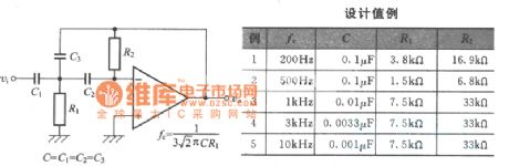
Multiple feedback type second-order bypass filter circuit diagram shown as follow:
(View)
View full Circuit Diagram | Comments | Reading(1623)
Using operational amplifier low-pass filter circuit diagram
Published:2014/3/24 21:22:00 Author:lynne | Keyword: Using operational amplifier low-pass filter circuit diagram

Using operational amplifier low-pass filter circuit diagram as shown:
Let R1 = R2, then the gain of the low frequency range 1 (= 0db). (View)
View full Circuit Diagram | Comments | Reading(1612)
Differential circuit diagram
Published:2014/3/23 21:35:00 Author:lynne | Keyword: Differential circuit diagram
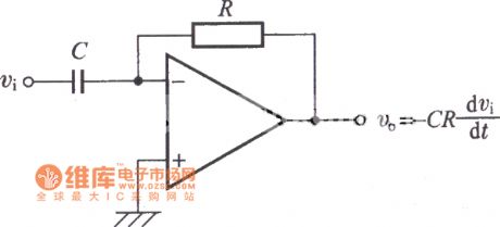
Differential circuit diagram as shown:
(View)
View full Circuit Diagram | Comments | Reading(1320)
The first-order bypass filter circuit diagram
Published:2014/3/23 21:34:00 Author:lynne | Keyword: The first-order bypass filter circuit diagram

The first-order bypass filter circuit diagram shown as follow:
(View)
View full Circuit Diagram | Comments | Reading(1767)
Add operation circuit diagram
Published:2014/3/23 21:33:00 Author:lynne | Keyword: Add operation circuit diagram
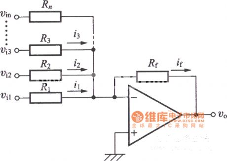
Add operation circuit diagram as shown:
(View)
View full Circuit Diagram | Comments | Reading(1475)
Integral circuit diagram
Published:2014/3/23 21:32:00 Author:lynne | Keyword: Integral circuit diagram
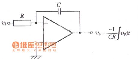
Integral circuit diagram shown as follow:
(View)
View full Circuit Diagram | Comments | Reading(1362)
Reverse amplification circuit diagram
Published:2014/3/23 21:06:00 Author:lynne | Keyword: Reverse amplification circuit diagram
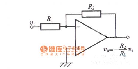
Reverse amplification circuit diagram as shown:
(View)
View full Circuit Diagram | Comments | Reading(1362)
| Pages:11/2234 1234567891011121314151617181920Under 20 |
Circuit Categories
power supply circuit
Amplifier Circuit
Basic Circuit
LED and Light Circuit
Sensor Circuit
Signal Processing
Electrical Equipment Circuit
Control Circuit
Remote Control Circuit
A/D-D/A Converter Circuit
Audio Circuit
Measuring and Test Circuit
Communication Circuit
Computer-Related Circuit
555 Circuit
Automotive Circuit
Repairing Circuit