
Circuit Diagram
Index 12
Synchronous rectifier adapter circuit 120W/12V/10A circuit diagram
Published:2014/3/20 21:03:00 Author:lynne | Keyword: Synchronous rectifier adapter circuit 120W/12V/10A circuit diagram,
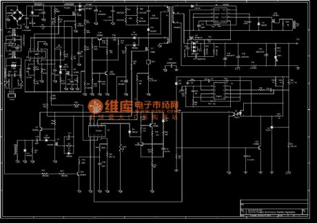
Synchronous rectifier adapter circuit 120W/12V/10A circuit diagram shown as following:
(View)
View full Circuit Diagram | Comments | Reading(2209)
Blown fuse alarm circuit diagram
Published:2014/3/20 20:44:00 Author:lynne | Keyword: Blown fuse alarm circuit diagram, VT66A, 2CW52

With this alarm can quickly determine if the fuse blows .WorksFuse alarm circuit as shown. When the fuse Fu intact , Fu ends of the same potential , C1 voltage at both ends of days , the alarm does not work. When Fu blown fuse , 220V AC by the load ( ie, appliances ) input current limit by the Rl buck , VD2 rectifier , C1 filtering and VD1 regulated output DC voltage of about 3V . This DC voltage supply music IC VT66A work on piezoelectric ceramics B loud electronic music newspaper tube sound, alerting the master fuse has blown .Component selection and productionMusic IC available VT66A Music transistor should be used in L-shaped , with each song name within the reservoir favorite may be. VD1 with 2cw52 regulator diode , VD2 1N4004 type silicon rectifier diodes are available .R1 with RJ-1W metal film resistors. C1 with CD11-10v electrolytic capacitor . L color code available 2.5mH inductor . B with FT-27, HTD27A-1 type and other piezoelectric ceramics .Entire alarm lines can be installed in a small plastic box , leads to two wires , it will be parallel to the ends of the fuse Fu .As shown in Figure blown fuse alarm circuit diagram:
(View)
View full Circuit Diagram | Comments | Reading(2215)
Low loss power supply of solar-powered light circuit diagram
Published:2014/3/20 21:02:00 Author:lynne | Keyword: Low loss power supply of solar-powered light circuit diagram, LM324, LM385
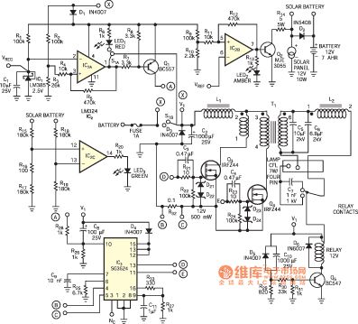
Solar lamp circuit is a low-loss circuit, using a four-pin 7W CFL (compact fluorescent lamps) and a 12V ,7-Ahr sealed maintenance-free batteries. Inverter efficiency greater than 85%, the quiescent current is less than 2mA. It has a protective function with battery discharge and overcharge protection feature parallel charge controller. Low quiescent current, over-discharge protection function and overcharge protection to ensure that the three very long battery life. Preheat function prevents the inverter CFL ends of black, thus extending its life. This circuit can be used as a reliable and compact portable light source in rural areas, in urban use as emergency light systems. Shunt charge controller circuit comprises IC1 (low current 2.5V voltage reference LM385) and IC2 (LM324 comparator). With resistors R1 ~ R8 and transistor Q1 IC2A prevent battery discharge. Solar-powered lights low-loss circuit diagram shown in Figure:
(View)
View full Circuit Diagram | Comments | Reading(5090)
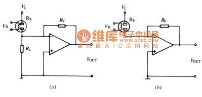
Zero-drift operational amplifier circuit diagrams
Published:2014/3/20 21:04:00 Author:lynne | Keyword: Zero-drift operational amplifier circuit diagrams,
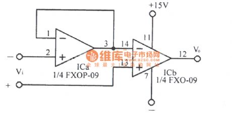
Zero-drift operational amplifier circuit diagram as shown:
(View)
View full Circuit Diagram | Comments | Reading(1669)
Zero drift inverting amplifier circuit diagrams
Published:2014/3/20 21:05:00 Author:lynne | Keyword: Zero drift inverting amplifier circuit diagrams,
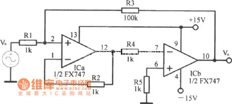
Zero drift inverting amplifier circuit diagrams shown as following:
(View)
View full Circuit Diagram | Comments | Reading(1540)
A3 (A4) power supply circuit
Published:2014/3/19 21:15:00 Author:lynne | Keyword: A3 (A4) power supply circuit, A3 (A4)
A3 (A4) power supply circuit shown as follow:
(View)
View full Circuit Diagram | Comments | Reading(4397)
SONY G3FK2 power circuit diagram
Published:2014/3/19 21:14:00 Author:lynne | Keyword: SONY G3FK2 power circuit diagram, G3FK2
SONY G3FK2 power circuit diagram shown as follow: (View)
View full Circuit Diagram | Comments | Reading(2859)
Enter 1.5 V to 22.5 V output circuit principle diagram
Published:2014/3/19 21:12:00 Author:lynne | Keyword: Enter 1.5 V to 22.5 V output circuit principle diagram,
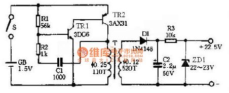
As shown is an output voltage 22.5V DC side of the booster circuit that can be used instead of 22.5V DC battery, which use a multimeter in a 1.5V battery-powered operating current of 25mA output current is about 0.5mA high barrier for Multimeter wealthy enough. circuit composed of complementary multivibrator TR1 and TR2, its oscillation frequency is approximately 2KHz.T is the primary line of step-up transformer load up multivibrator secondary liters a high voltage output voltage of the pulse wave which the voltage after the rectifier diode D1 and the capacitor C2 becomes wave DC high voltage, and then after the resistor R3 and the voltage regulator tube ZD1 can output a stable high voltage.
(View)
View full Circuit Diagram | Comments | Reading(5845)
Small DC booster circuit diagram
Published:2014/3/19 21:09:00 Author:lynne | Keyword: Small DC booster circuit diagram,
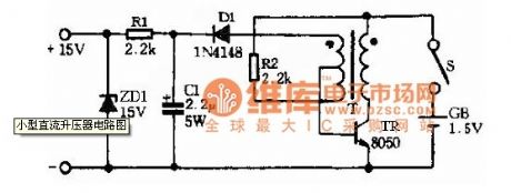
Small DC booster circuit diagram as shown:
(View)
View full Circuit Diagram | Comments | Reading(1789)
The output voltage of the op amp circuit diagram
Published:2014/3/19 21:15:00 Author:lynne | Keyword: The output voltage of the op amp circuit diagram,


The output voltage of the op amp circuit diagram shown as follow:
(View)
View full Circuit Diagram | Comments | Reading(1421)
Dongfeng Peugeot Citroen Picasso 2.0L sedan electric mirrors Diagram
Published:2014/3/18 21:15:00 Author:lynne | Keyword: Dongfeng Peugeot Citroen Picasso 2.0L sedan electric mirrors Diagram,
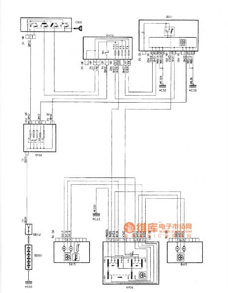
Dongfeng Peugeot Citroen Picasso 2.0L sedan electric mirrors Diagram shown as follow:
(View)
View full Circuit Diagram | Comments | Reading(1402)
Tl494 inverter circuit diagram
Published:2014/3/18 21:17:00 Author:lynne | Keyword: Tl494 inverter circuit diagram, Tl494
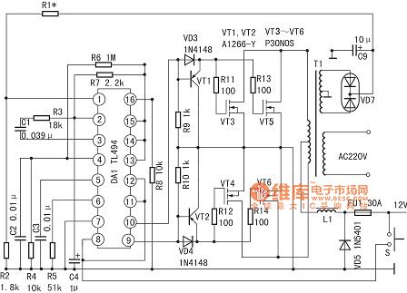
Tl494 inverter circuit diagram as shown:
(View)
View full Circuit Diagram | Comments | Reading(6977)
Inverter power supply circuit diagram
Published:2014/3/18 21:19:00 Author:lynne | Keyword: Inverter power supply circuit diagram,
Inverter power supply circuit diagram shown as follow:
(View)
View full Circuit Diagram | Comments | Reading(5090)
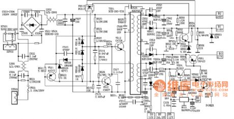
Switching power supply circuit diagram
Published:2014/3/18 21:19:00 Author:lynne | Keyword: Switching power supply circuit diagram
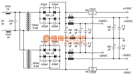
Switching power supply circuit diagram as shown:
(View)
View full Circuit Diagram | Comments | Reading(3516)
Gas sensor resistance with temperature schematic
Published:2014/3/18 21:22:00 Author:lynne | Keyword: Gas sensor resistance with temperature schematic,
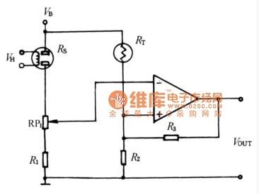
Gas sensor resistance changes with temperature thermistor can be applied with similar characteristics to compensate for temperature. Figure 8-17 shows a bridge circuit connected to the gas sensor temperature compensation circuit, the circuit is also access to a comparator with hysteresis. Signal magnitude adjustment variable resistor RP1. When applied to the inverting input terminal of the voltage exceeds a threshold level of the upper limit, the output level is set at a low level. The reverse voltage is applied before the input level is lower than the threshold voltage, the high level of the output terminal is disposed, so as to significantly reduce the need for appropriate measurement when the concentration of gas.
(View)
View full Circuit Diagram | Comments | Reading(2392)
Dongfeng Peugeot Citroen Picasso 2.0L sedan speeding alarm buzzer circuit diagram
Published:2014/3/17 21:39:00 Author:lynne | Keyword: Dongfeng Peugeot Citroen Picasso 2.0L sedan speeding alarm buzzer circuit diagram,
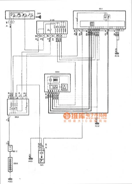
Dongfeng Peugeot Citroen Picasso 2.0L sedan speeding alarm buzzer circuit diagram as shown:
(View)
View full Circuit Diagram | Comments | Reading(2097)
RC Buck power supply circuit
Published:2014/3/17 21:38:00 Author:lynne | Keyword: RC Buck power supply circuit,
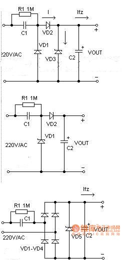
Conventional methods AC power is converted to low voltage DC rectifier filter before using the step-down transformer, when restrictions on the size and cost factors, the most simple and practical method is to use capacitor step-down power supply.
First, the circuit schematic
Simple basic buck power supply circuit capacitance in Fig, C1 is a step-down capacitor, D2 for the half-wave rectifier diode, D1 in the negative half cycle of the mains to provide a discharge circuit C1, D3 is a Zener diode, R1 is power off After the charge C1 bleeder resistor. Is often used in practical applications of the circuit shown in Figure 2. When the need to provide a larger load current, the bridge rectifier circuit can be used as shown in Figure 3.
Unregulated rectified DC voltage is generally higher than 30 volts, and will vary with changes in load current large fluctuations occur, it is because a lot of the reason of such power due to internal resistance, it is not suitable for high current power supply applications.
Conventional methods AC power is converted to low voltage DC rectifier filter before using the step-down transformer, when restrictions on the size and cost factors, the most simple and practical method is to use capacitor step-down power supply.
First, the circuit schematic
Simple basic buck power supply circuit capacitance in Figure 1, C1 is a step-down capacitor, D2 for the half-wave rectifier diode, D1 in the negative half cycle of the mains to provide a discharge circuit C1, D3 is a Zener diode, R1 is off C1 charge after power bleeder resistors. Is often used in practical applications of the circuit shown in Figure 2. When the need to provide a larger load current, the bridge rectifier circuit can be used.
Unregulated rectified DC voltage is generally higher than 30 volts, and will vary with changes in load current large fluctuations occur, it is because a lot of the reason of such power due to internal resistance, it is not suitable for high current power supply applications.
Second, the device selection
1 circuit design, the exact value should be measured load current, and then select the reference sample capacity buck capacitor. Because the capacitor C1 through the buck to the load current Io, flowing C1 actually charge and discharge current Ic. C1 greater capacity, the smaller the capacitive reactance Xc, then flows through C1 charge and discharge current increases. When the load current Io is less than C1 charge and discharge current, the excess current will flow through the regulator, if the regulator is less than the maximum allowable current Idmax Ic-Io when the regulator could easily lead to burnout.
(2) To ensure reliable operation of C1, the pressure should be chosen to be greater than twice the supply voltage.
3 bleeder resistor R1 must be selected to ensure that within the required time exhausting the charge on C1.
Third, the design example
Known C1 is 0.33μF, AC input 220V/50Hz, seeking circuit can supply a maximum current load. C1 reactance Xc in the circuit is:
Xc = 1 / (2 πf C) = 1 / (2 * 3.14 * 50 * 0.33 * 10-6) = 9.65K
Flows through the capacitor C1 of the charging current (Ic) is:
Ic = U / Xc = 220 / 9.65 = 22mA.
Capacitor C1 is often the relationship between blood pressure and the load current Io capacitance C can be approximated that: C = 14.5 I, where C is the capacity of the unit is μF, Io unit is A. Capacitor Buck is a non-isolated power supply, pay special attention to the application of isolation, to prevent electric shock.
RC Buck power supply circuit shown in Fig. :
(View)
View full Circuit Diagram | Comments | Reading(4590)
Sine wave inverter circuit diagram
Published:2014/3/17 21:29:00 Author:lynne | Keyword: Sine wave inverter circuit diagram, ICL7660, MAX1044
Existing inverter, well-sine wave output and output. High efficiency inverter square wave output, but are designed for the electrical sine wave power, the use is not always assured, although you can apply to many appliances, but some appliances do not apply, or electrical indicators up change. Sine wave output inverter no shortcomings in this area, but there is the disadvantage of low efficiency. Designed a highly efficient sine wave inverter, the circuit shown in Figure 1.
The circuit is powered by a 12V battery. First with a voltage doubler amplifier module times the pressure of supply. Can select ICL7660 or MAX1044. Op amp a 50Hz sine wave as a reference signal generated. 2 op amp as an inverter. 3 and op amp op amp as a comparator with hysteresis 4. In fact, the op amp 3 and switch a proportion of the switching power supply is constructed. Operational amplifier 4 and switch 2 also. Its switching frequency is unstable. In the op-amp output signal is positive phase, the op amp 3 and switch jobs. Then the output of op amp 2 is negative phase. Then the positive input of operational amplifier 4, the potential (fixed to 0) than the high potential of the negative input, the output of operational amplifier 4 is a constant, the switch is closed. In an op-amp output is negative phase, the opposite. This enables the two switches alternately work.
Below is a discussion about how the switch works. When the reference signal is less than the detection signal, that is the amplifier negative input terminal 3 or 4 signal is high a small value than the positive input signal, the comparator outputs 0, the switch opened, followed detection signal rapidly increased, when the detection signal higher than the reference value of a tiny signal, the comparator output 1, switch off. It should be noted here that, in the comparator circuit has a flip positive feedback, which is a hysteresis characteristic of the comparator. For example, under the reference signal is lower than the detection signal of the premise, as they continue to close the difference, at the moment they are equal, the reference signal detection signal immediately higher than a certain value. This certain value affect the switching frequency. The lower it is the greater frequency. Here choose it for the 0.1 ~ 0.2V.
C3, C4 role is to allow a high frequency current through the freewheeling switch, while the low-frequency impedance greater 50Hz signal. C5 by the equation: 50 = calculated. L is generally 70H, the production is best measured it. Thus C is about 0.15μ. The ratio of R4 and R3 should be strictly equal to 0.5, significantly larger waveform distortion, small start-up can not be, but rather a number of large, non-small. Maximum current switch is: I == 25A.
Click here for a more detailed discussion of selected values of L1, L2's. Equivalent to the load back to the input side of the transformer, the circuit of Figure 2.
Considering the switching frequency is much greater than 50Hz , the switch from on to off in the process , you can put a voltage transformer as a constant. The output of the power energy of the L : W = ∫ Uccdt = t
Ignore all the loss is not ideal , this energy should be equal to the load energy consumption . The average power of the formula : P == t
I hope when Ucc-U is close to a small value, the battery can be higher switching frequencies and to meet the requirements of the transformer. This a little value here take 0.5V, the frequency of taking 5kHz. When Ucc-U <0.5V, the switch will open a long time (which is relatively a ) . If you need the power of the maximum output power of 150W, then the load resistance is 322.7Ω, converted to the transformer input is : 0.48 Ω.
∴ instantaneous load power at this time is : P == 276W∴ P = × = 276∴ L = 2.2μH
L value can be seen in small disadvantage for the switch , and the output is clipping . You can increase the production of L values, but the maximum output power will be reduced. The best way to solve this problem is to use 16V power supply , the transformer is also used 8.5V (peak to 12V), and the peak for the reference signal of 12V , but this time the need to change the circuit . (View)
View full Circuit Diagram | Comments | Reading(2584)
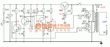
High power regulator inverter circuit diagrams
Published:2014/3/17 21:22:00 Author:lynne | Keyword: High power regulator inverter circuit diagrams, TL494, 2SK906, 2SK564
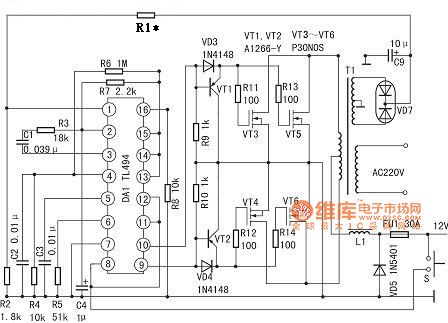
The use of the composition of 400W power regulator TL494 inverter circuit. It excited transform part is TL494, VT1, VT2, VD3, VD4 constitutes a sink current drive circuit, driving two of each two 60V/30A MOS FET switch. For increasing the output power of each channel can be three to four switches in parallel applications, the circuit unchanged. The inverter TL494 application as follows:
1,2 feet constituted regulator sampling error amplification system, a positive input pin input sampling secondary winding rectifier inverter output 15V DC voltage, the R1, R2 partial pressure, so that the first leg of the inverter Nearly 4.7 ~ 5.6V voltage sampling work. Inverting input pin 2 Input 5V reference voltage (from 14 feet out). When the output voltage is reduced, a lower pin voltage error amplifier output low, the PWM circuit output voltage increases. When a voltage is normal foot 5.4V, 2-pin voltage is 5V, 3-pin voltage is 0.06V. Then the output AC voltage is 235V (square-wave voltage). 4-pin external R6, R4, C2 set the dead time. Normal voltage is 0.01V. 5,6 pin external CT, RT triangle wave oscillator frequency is set to 100Hz. 5 pin voltage is normal 1.75V, 6-pin voltage is 3.73V. 7 feet for common ground. 8, 11 feet inside the drive output transistor collector, 12 feet for the TL494 pre-supply terminal, this three-terminal controlled by a switch S TL494 start / stop, as the inverter control switch. When S1 is turned off, TL494 no output pulse, so the switch VT4 ~ VT6 no current. When S1 is turned on, this tripod is the battery voltage is positive voltage. 9,10 feet inside the driver stage transistor emitter output two different positive pulse timing. Normal voltage is 1.8V. The first 13, 14 feet 14 feet 5V reference voltage output, so that there is 5V 13 feet high, the control gates, flip-flop output two drive pulses, for push-pull switching circuits. The first 15-pin external 5V voltage, constitute the reference voltage error amplifier inverting input to the non-inverting input terminal 16 feet high protection constitute input. In this connection, when the input is greater than 16 feet high of 5V, the output voltage can be reduced through the role of regulator, on or off the drive pulses to achieve protection. In its excited inverter output is almost no possibility of overpressure, so the circuit is not used in the first 16 feet, the ground by a resistor R8.
The capacity of 400VA inverter with power frequency transformer cores using 45 × 60mm2 silicon steel. The primary winding of wire with a diameter of 1.2mm, two and around 2 × 20 turns. Secondary sampling using 0.41mm wire winding around the 36-turn, center tap. 230V secondary winding is calculated by using the 0.8mm enameled wire wound 400 turns. Switch VT4 ~ VT6 available 60V/30A any type of N-channel MOS FET tube instead. VD7 available 1N400X series ordinary diodes. The circuit is almost without debugging to work properly. When C9 positive terminal voltage is 12V, R1 can be between 3.6 ~ 4.7kΩ choice, or 10kΩ potentiometer is adjusted so that the output voltage rating. If this is the inverter output power increases almost 600W, the primary current in order to avoid excessive increase of the resistive losses, should the battery switch to 24V, VDS can be used to switch high current MOS FET 100V tube. It should be noted that the choice of multi-tube rather parallel, rather than choose single IDS greater than 50A of the switch, the reason is: a higher price, two driving too difficult. Suggested the use of 100V/32A of 2SK564, 2SK906 or optional three parallel applications. Meanwhile, the transformer core cross section required to achieve 50cm2, calculated by the ordinary power transformer turns and calculated diameter, or the use of alternative waste transformer UPS-600. Such as refrigerators, electric fans powered, do not forget to join LC low-pass filter.
Power regulator inverter circuit shown in Figure:
> (View)
View full Circuit Diagram | Comments | Reading(9269)
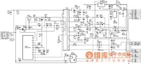
3844 switching power supply circuit
Published:2014/3/17 20:59:00 Author:lynne | Keyword: 3844 switching power supply circuit,
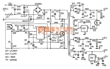
3844 switching power supply circuit shown as follow: (View)
View full Circuit Diagram | Comments | Reading(4862)
| Pages:12/2234 1234567891011121314151617181920Under 20 |
Circuit Categories
power supply circuit
Amplifier Circuit
Basic Circuit
LED and Light Circuit
Sensor Circuit
Signal Processing
Electrical Equipment Circuit
Control Circuit
Remote Control Circuit
A/D-D/A Converter Circuit
Audio Circuit
Measuring and Test Circuit
Communication Circuit
Computer-Related Circuit
555 Circuit
Automotive Circuit
Repairing Circuit