
Circuit Diagram
Index 10
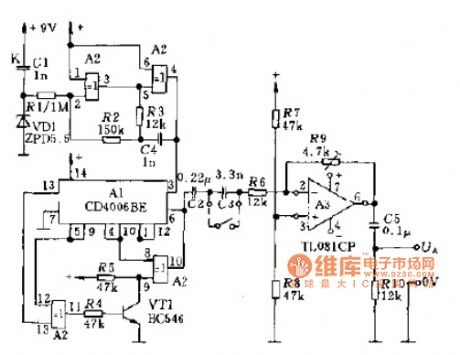
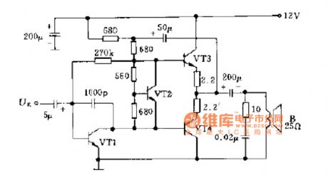
A voice control recording circuit diagram
Published:2014/4/1 21:26:00 Author:lynne | Keyword: A voice control recording circuit diagram
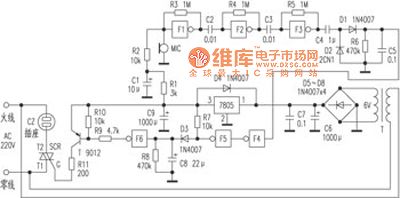
When a sound wave compression electret microphone MIC, MIC can output a weak audio signal fed from the NAND gate F1, F2, F3 and R3, R4, R5 constitute the three continuous linear amplification of the amplifier circuit , if consider peak waveform distortion , the output signal amplitude F3 has been large enough , after this signal is coupled through C4 by D1, D2 rectifier get unipolar pulses C5 charging. VC5 soon more than 1/2VDD, the output of NAND gate F4 0, F5 output is 1 , high charge to C8, VC8 also soon be greater than 1/2VDD, F6 output is 0 , the transistor T saturated conduction , SCR is trigger , so 220V mains supply via socket CZ to the recorder , recording starts ; If the sound disappears, the C5 voltage can not be maintained , VC5 quickly dropped to zero. Similarly , C8 only slowly discharge to R8, VC8 about three seconds after the drop to 0 , then , SCR deadline , tape recorders recording aborted ; so, automatic recording control recording ( if necessary delay longer available appropriate to increase the capacity of C8 ) .
This control circuit is not only used for automatic recording recorder can also be extended to other appliances require intermittent voice, interested friends can do it. If the sensitivity is not satisfied, it can be in F1 before adding a transistor amplifier.
(View)
View full Circuit Diagram | Comments | Reading(1746)
The thyristor ac voltage regulation circuit diagram
Published:2014/4/1 21:19:00 Author:lynne | Keyword: The thyristor ac voltage regulation circuit diagram
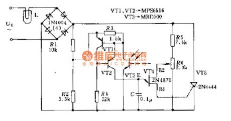
In order to stabilize the circuit diagram lamp brightness L, using thyristor AC automatic voltage regulator is the way, for access thyristor T5 on a diagonal line from the bridge of exchanges. Their trigger pulse generated by a single-junction transistor VT4. Transistor VT1 . VT2 and VT3 phototransistor play the role of the equivalent resistance when the lamp light due to supply voltage change, the change in resistance phototransistor, single-junction transistor control voltage phase also changed, so that the trigger pulse phase thyristor move, increase or decrease the thyristor time, the voltage on the approximation of L remains unchanged. brightness of the projector lamp is also approximately unchanged. makes light stability. The AC thyristor regulator circuit diagram shown in Fig.
(View)
View full Circuit Diagram | Comments | Reading(4125)
Light control switch circuit schematic
Published:2014/4/1 21:18:00 Author:lynne | Keyword: Light control switch circuit schematic
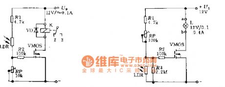
Using the sensor can be used for the power MOS FET power switch, the switch can be used photoresistor LDR. When light is irradiated onto the photosensitive resistor, LDR low resistance, a signal is applied to the gate of the field effect transistor off, the source and drain between conduction from the surface of the relay coil K changes state, for generating control signals, or, if connected to the photoresistor LDR at the low potential, in the dark when no light is irradiated onto the photosensitive resistor, with the photosensitive resistor. Light control switch circuit diagram shown in Fig.
(View)
View full Circuit Diagram | Comments | Reading(2674)
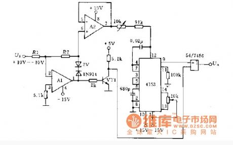
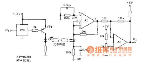
Infrared remote monitoring circuit schematic
Published:2014/4/1 21:17:00 Author:lynne | Keyword: Infrared remote monitoring circuit schematic
Infrared remote monitoring circuit schematic shown as follow:
(View)
View full Circuit Diagram | Comments | Reading(2306)
Signal repeater circuit diagram
Published:2014/4/1 21:16:00 Author:lynne | Keyword: Signal repeater circuit diagram
Signal repeater circuit diagram as shown:
(View)
View full Circuit Diagram | Comments | Reading(2401)
Switch Timing Circuit Diagram
Published:2014/3/31 21:33:00 Author:lynne | Keyword: Switch Timing Circuit Diagram
Switch Timing Circuit Diagram shown as follow:
(View)
View full Circuit Diagram | Comments | Reading(2187)
Light control relay circuit diagram
Published:2014/3/31 21:32:00 Author:lynne | Keyword: Light control relay circuit diagram
Light control relay circuit diagram as shown:
(View)
View full Circuit Diagram | Comments | Reading(2393)
Analog switch circuit schematic
Published:2014/3/31 21:31:00 Author:lynne | Keyword: Analog switch circuit schematic
Analog switch circuit schematic shown as follow:
(View)
View full Circuit Diagram | Comments | Reading(2176)
Transmission of data coupling circuit diagram
Published:2014/3/31 21:27:00 Author:lynne | Keyword: Transmission of data coupling circuit diagram
Transmission of data coupling circuit diagram shown as follow:
(View)
View full Circuit Diagram | Comments | Reading(1451)
FAW Hongqi buzzer system schematics
Published:2014/3/31 21:30:00 Author:lynne | Keyword: FAW Hongqi buzzer system schematics
FAW Hongqi buzzer system schematic as shown:
(View)
View full Circuit Diagram | Comments | Reading(1373)
Noise generator circuit schematics
Published:2014/3/30 21:30:00 Author:lynne | Keyword: Noise generator circuit schematics
Noise generator circuit schematics shown as follow:
(View)
View full Circuit Diagram | Comments | Reading(1815)
Speech filter circuit diagram
Published:2014/3/30 21:24:00 Author:lynne | Keyword: Speech filter circuit diagram
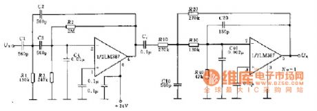
Speech filter circuit diagram as shown:
(View)
View full Circuit Diagram | Comments | Reading(2010)
Loudspeaker overload protection circuit diagram
Published:2014/3/30 21:22:00 Author:lynne | Keyword: Loudspeaker overload protection circuit diagram
Loudspeaker overload protection circuit diagram shown as follow:
(View)
View full Circuit Diagram | Comments | Reading(2486)
Signal generator circuit diagram
Published:2014/3/30 21:21:00 Author:lynne | Keyword: Signal generator circuit diagram
Signal generator circuit diagram as shown:
(View)
View full Circuit Diagram | Comments | Reading(1398)
Thyristor controlled motor reversing circuit diagram
Published:2014/3/30 21:07:00 Author:lynne | Keyword: Thyristor controlled motor reversing circuit diagram
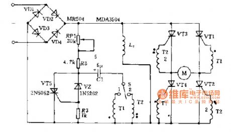
Thyristor controlled motor reversing circuit diagram shown as follow:
(View)
View full Circuit Diagram | Comments | Reading(3002)
Made of 5 ma PNP transistor constant current source bridge type pressure sensor power supply circuit principle diagram
Published:2014/3/27 21:26:00 Author:lynne | Keyword: Made of 5 ma PNP transistor constant current source bridge type pressure sensor power supply circuit principle diagram
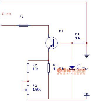
Made of 5 ma PNP transistor constant current source bridge type pressure sensor power supply circuit principle diagram shown as follow:
(View)
View full Circuit Diagram | Comments | Reading(3616)
One-touch switching power supply circuit
Published:2014/3/27 21:24:00 Author:lynne | Keyword: One-touch switching power supply circuit
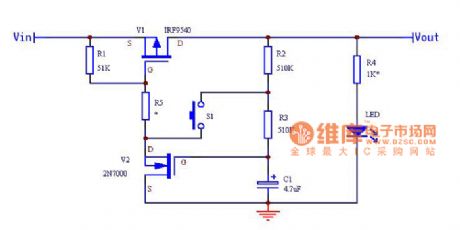
This circuit can be applied to a wide range of voltages (4.5V ~ 40V, the maximum current of 19A ), R5 is optional , when the input voltage is less than 20V can be short-circuited ; greater than the input voltage by connecting the 20V, R5 values R1 should meet with the partial pressure of the MOS GS voltage of V1 is less than greater than -20V -5V ( V2 when conduction ) as possible, the voltage V1 at the GS between ~-20V -10V so that a large current output V1 .Before the button is pressed , GS voltage V2 (ie C1 voltage ) is zero , V2 deadline , V1 , GS voltage is 0, V1 cut no output ; When you press S1, C1 charging , V2 GS voltage rises to about 3V when V2 guide pass and quickly saturated , V1 GS voltage is less than -4V, V1 saturated conduction , Vout with output, LED light ( and you should release the button ) C1 through R2, R3 continue to charge , V1, V2 state is locked ; when pressed again The next button , because V2 is saturated conduction state, the drain voltage of approximately 0V, C1 discharges through R3 , when put to approximately 3V , V2 deadline , V1 gate-source voltage is greater than -4V, V1 cut , Vout no output , LED tube off ( release button ), C1 through R2, R3 , and continues to be discharged outside of the circuit , V1, V2 to maintain the off state.Note : S1 makes Vout should be open or closed after the button is released , or will form the switching oscillation.One-touch switching power supply circuit shown in Fig.
(View)
View full Circuit Diagram | Comments | Reading(5368)
Single power supply switch plus or minus power circuit diagram
Published:2014/3/27 21:23:00 Author:lynne | Keyword: Single power supply switch plus or minus power circuit diagram, CD4069
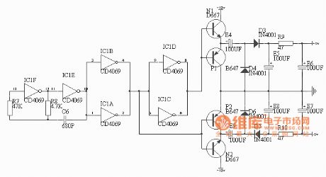
General Electric sound work, the need to provide positive and negative power. But in cars, boats, trains and other vehicles can only use battery power, a power supply circuit here, we want to help. The power from the oscillator circuit, inverter, rectifier and pusher and components such as filters, the circuit works as shown
Oscillator
This is a typical CMOS gate by (CD4069) constitute oscillator. Shock accuracy of 10-2 to 10-3, the shock process is as follows: Let the circuit at a time point B is high then the AB point to charge the capacitor through a resistor R8. The beginning of charging, the voltage across the capacitor is not due mutation, making the C point mutation to high potential, with the charge of conduct, C point potential gradually decreased. When the C-point conversion potential is lower than the voltage CMOS NAND gate, NAND gate 41F flip, A point goes high, B point becomes low. Since the voltage across the capacitor is not mutated, making the C point mutation to low potential. A point to the capacitor through a resistor R8 C6 reverse charge. With the charge carried, C point potential gradually increased when the C-point potential is higher than the conversion voltage CMOS NAND gate, NAND gate 41F flip, A point goes low, B point is to charge the capacitor through a resistor R8 C6 ...... repeating the above procedure, the formation of oscillation, the output pulse voltage at the point B. This oscillation frequency is f = 1/2ΠR8C6 = 1/2 * 3.14 * 4.7 * 103 * 680 * 10-12 = 49.8KHz, duty cycle 2. Figure resistor R7 (47K) Average value of R7 = (5 ~ 10) R8, its role is twofold: 1) to reduce the impact of power supply variations on the oscillation frequency. 2) reduce dynamic power circuits work.
Inverters
Divided into two groups of four inverters, respectively, opposite phase output pulse voltage, which pairwise parallel to increase the output current (SLR maximum output current of 1.5 mA, the shunt can output 3 mA). Advantages of CMOS inverters are: anti-interference ability, wide supply voltage range (3 ~ 20V), just apply to this circuit, the power of the circuit is 18V.
Pusher
Look at the two transistors N1 and P1 works, N1 consisting of common collector amplifier circuit for amplifying the input pulse voltage signal positive half cycle; P1 is also composed of common collector amplifier circuit for amplifying the negative half cycle of the input pulse voltage signal, they synthesized output phase with the input signal phase at point E, but opposite current amplification (up to two or three times) pulse voltage signal. Two transistors N2 and P2 with the working principle is similar, but the phase of the pulse signal and the voltage signal output from the point E to point F in opposite output, a rectifying circuit for the following positive and negative voltages, respectively, the entire effluent. In this circuit, the two transistors selection D647, D667, its argument is: 0.9w, +1 A/-1A.
Rectifier and filter
This part of the circuit is very classic, although voltage doubling rectifier circuit, but the loss due to other reasons, in this circuit when the load is +12 V/-12V, rated load +9 V/-9V. This power supply circuit provides power less than 11W.
Further, in the practical application of the circuit, the oscillation signal of the presence of 50KHZ, note frequency shielding, such as a printed board with this part of the circuit enclosed foil shielding. In addition, the power supply ripple factor depending on the desired single-supply ripple. Since the commissioning of the project power is not available, so long as the part is good, the connection is correct, it can work properly.
Single power converter shown in Figure positive and negative power supply circuit
(View)
View full Circuit Diagram | Comments | Reading(5541)
Dual polarity power supply circuit diagram
Published:2014/3/27 21:21:00 Author:lynne | Keyword: Dual polarity power supply circuit diagram,
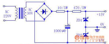
Dual polarity power supply circuit diagram as shown:
(View)
View full Circuit Diagram | Comments | Reading(4707)
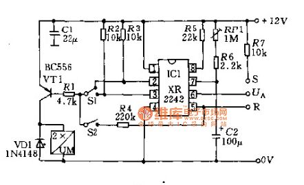
Several commonly used backup power supply circuit diagram
Published:2014/3/27 21:20:00 Author:lynne | Keyword: Several commonly used backup power supply circuit diagram, MC34164, LM2931T, ICL7673, MAX610, LM2935
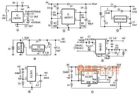
Here are a few dedicated uninterruptible power supply circuit, especially for low-power or batteries places. Can be used as a backup power source other low-voltage power circuit memory, microprocessors, CMOS circuits, timer and calendar clock circuit.
Self-based backup regulator
LM2935 is a low drop voltage regulator, in addition to a +5 V/750mA regulated output, the internal device also has a low quiescent backup regulator, its normal output is +5 V/10mA, Figure 1 shows a typical wiring LM2935 Figure. Backup function mainly regulator in the line when subjected to transient shocks (such as line input suddenly reaches 60V voltage exceeds the maximum input voltage transient limit), 750mA regulator output will automatically shut down to protect the internal circuitry and load, but still normal backup regulator output, as long as the reset level and ultra-low input voltage does not occur simultaneously, it can make a backup storage without data loss of normal power supply.
Power failure backup regulator circuit
Although low dropout regulator LM2931T just a battery regulator, using it as a power failure backup is very convenient. The circuit in Figure 2 when the normal power supply, input output directly through D3, D1 and R1 also by Ec backup battery trickle charge, LM2931T is high and 2 feet off the output; When the line when the input power failure, LM2931T 2 feet will be low, the output power to the load through D4 continued regulation. Backup circuit can accommodate a wide range of voltages, power regulator RP obtain suitable output circuit for the isolation diodes D1-D4, the best selection of low drop Schottky diode.
Backup power boost switch IC
RH5RCXXX series circuit is a three-terminal regulator IC CMOS switch, low current consumption of only 7.5uA. As long as the input voltage is greater than 0.9V, the boost switch output can be achieved, the conversion efficiency is generally above 80%. The circuit in Figure 3 constitutes a use RH5RCXX clamp boost backup power. The main power supply circuit E1, E2 as an auxiliary power when the main power output strong, diode D2 deadline, RH5RCXX boost circuit does not work; When the main power is turned down to D2, E2 will D1 auxiliary power off switch boost Backup power output circuit. Figure 4 is a power-saving backup power circuit. At higher battery voltage, output voltage detector 1 foot MC34164 blocking, V cutoff, power Ec directly through L, D1 output; supply Ec voltage drop is detected when IC1 effective, a pin output low, the end of the suction current of about 6mA, it was R so that V conduction, allowing the boost switch circuit, the battery Ec may continue to be used.
Transformerless power backup
With MAX's electricity converter MAX610 can constitute a +5 V uninterruptible power supplies, backup batteries use ultracapacitors. Under normal circumstances 2,8 feet rectified output of the IC through R3 backup battery trickle charge current is selected as the best one-tenth or less of battery capacity. When power cut, D conduction, so Ec by internal series regulator IC output freewheeling, the maximum output current up to 150mA, to ensure that the load is not power-down operation. It is noteworthy that the best choice of diode Schottky diode D, such as D83004, etc., buck capacitor C2 should have a withstand voltage of 450V or more, when the electricity is when 220V/50Hz, R1 take 100 ohms; When the mains voltage is When 110V/60Hz, R1 taken 47 ohm.
ASIC backup power
ICL7673 is a monolithic CMOS ASIC-based backup power can achieve output 2.5-15V input voltage range of backup power, then the normal power supply pin Vp, Vs take a backup power supply, power supply was normal Pbar bottom level, and Sbar blocking ; when energized,, Pbar blocked, and Sbar bottom level output; supply of +5 V when the output current is 38mA, when the power supply 3V, the output current is 30mA, Sbar and Pbar end load capacity of about 50mA. Small power backup power supply 6 is constituted by the ICL7673, spare battery with 3.6V lithium battery or super capacitor bank. When normal power supply, battery trickle charge to get. +5 V power failure, +3.6 V output will freewheeling diode D prevents backflow backup battery power is consumed in the normal end; To accommodate large load backup ICL7673, and Figure 7 pipe expansion flow output by PNP, V1 under normal circumstances lead Tong, V2 at the time of the backup power supply is turned on.
Several commonly used backup power supply circuit shown in Figure
(View)
View full Circuit Diagram | Comments | Reading(4950)
| Pages:10/2234 1234567891011121314151617181920Under 20 |
Circuit Categories
power supply circuit
Amplifier Circuit
Basic Circuit
LED and Light Circuit
Sensor Circuit
Signal Processing
Electrical Equipment Circuit
Control Circuit
Remote Control Circuit
A/D-D/A Converter Circuit
Audio Circuit
Measuring and Test Circuit
Communication Circuit
Computer-Related Circuit
555 Circuit
Automotive Circuit
Repairing Circuit