
Circuit Diagram
Index 9
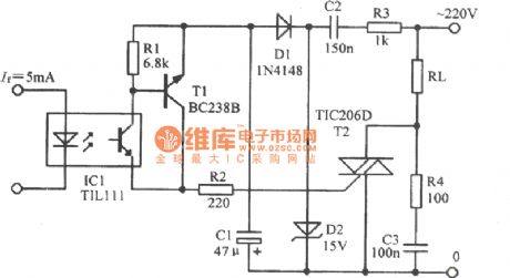
Promote grounding load large current negation gate circuit diagram
Published:2014/4/8 21:13:00 Author:lynne | Keyword: Promote grounding load large current negation gate circuit diagram
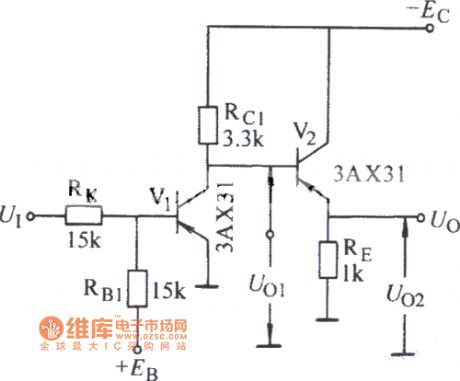
Promote grounding load large current negation gate circuit diagram shown as follow:
(View)
View full Circuit Diagram | Comments | Reading(1433)
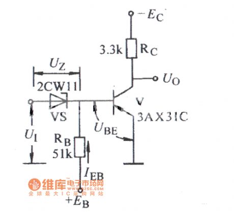
Zener diode clamping of the gate circuit diagram
Published:2014/4/8 21:07:00 Author:lynne | Keyword: Zener diode clamping of the gate circuit diagram
Zener diode clamping of the gate circuit diagram as shown:
(View)
View full Circuit Diagram | Comments | Reading(1443)
Output has a clamp diode gate circuit diagram
Published:2014/4/8 21:01:00 Author:lynne | Keyword: Output has a clamp diode gate circuit diagram
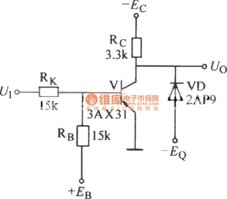
Output has a clamp diode gate circuit diagram shown as follow:
(View)
View full Circuit Diagram | Comments | Reading(1298)
Ordinary diode threshold gate circuit diagram
Published:2014/4/8 20:59:00 Author:lynne | Keyword: Ordinary diode threshold gate circuit diagram
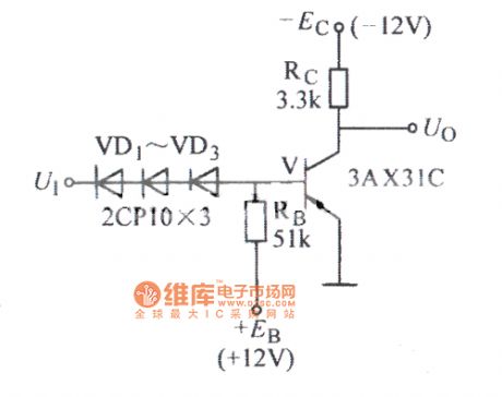
Ordinary diode threshold gate circuit diagram as shown:
(View)
View full Circuit Diagram | Comments | Reading(2288)
Threshold NAND gate with a front level gate resistance circuit diagram
Published:2014/4/8 20:53:00 Author:lynne | Keyword: Threshold NAND gate with a front level gate resistance circuit diagram
Threshold NAND gate with a front level gate resistance circuit diagram shown as follow:
(View)
View full Circuit Diagram | Comments | Reading(1489)
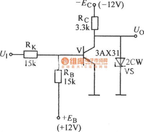
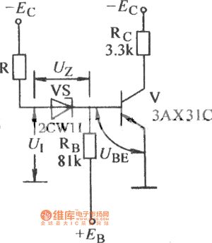
Voltage-regulator diode threshold gate circuit diagram
Published:2014/4/7 21:37:00 Author:lynne | Keyword: Voltage-regulator diode threshold gate circuit diagram
Voltage-regulator diode threshold gate circuit diagram shown as follow:
(View)
View full Circuit Diagram | Comments | Reading(2689)
The digital circuit composed of amplifier circuit diagram
Published:2014/4/7 21:36:00 Author:lynne | Keyword: The digital circuit composed of amplifier circuit diagram
The digital circuit composed of amplifier circuit diagram as shown:
(View)
View full Circuit Diagram | Comments | Reading(1452)
Oscillator (ceramic) infrared emission circuit principle diagram
Published:2014/4/7 21:35:00 Author:lynne | Keyword: Oscillator (ceramic) infrared emission circuit principle diagram
Oscillator (ceramic) infrared emission circuit principle diagram shown as following:
(View)
View full Circuit Diagram | Comments | Reading(1328)
MC1488 circuit diagram
Published:2014/4/7 21:33:00 Author:lynne | Keyword: MC1488 circuit diagram, MC1488
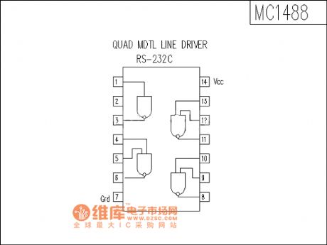
MC1488 circuit board as shown:
(View)
View full Circuit Diagram | Comments | Reading(2674)
Sail power sunroof circuit diagram
Published:2014/4/7 21:31:00 Author:lynne | Keyword: Sail power sunroof circuit diagram
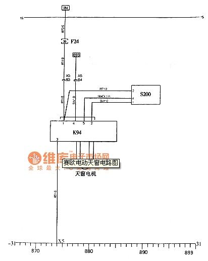
Sail power sunroof circuit diagram shown as follow:
(View)
View full Circuit Diagram | Comments | Reading(1453)
FM receiver circuit diagram
Published:2014/4/3 20:45:00 Author:lynne | Keyword: FM receiver circuit diagram
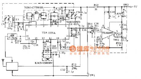
FM receiver circuit diagram shown as follow:
(View)
View full Circuit Diagram | Comments | Reading(1882)
Thyristor drive amplifier circuit diagram
Published:2014/4/3 20:44:00 Author:lynne | Keyword: Thyristor drive amplifier circuit diagram
Thyristor drive amplifier circuit diagram as shown:
(View)
View full Circuit Diagram | Comments | Reading(2086)
Phonograph amplifier circuit diagram
Published:2014/4/3 20:41:00 Author:lynne | Keyword: Phonograph amplifier circuit diagram
Phonograph amplifier circuit diagram shown as follow:
(View)
View full Circuit Diagram | Comments | Reading(1777)
High-voltage amplification circuit diagram of SCR
Published:2014/4/3 20:39:00 Author:lynne | Keyword: High-voltage amplification circuit diagram of SCR
High-voltage amplification circuit diagram of SCR as shown:
(View)
View full Circuit Diagram | Comments | Reading(1969)
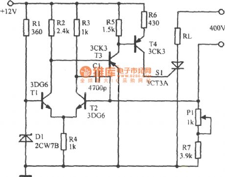
Sail anti-theft system circuit diagram
Published:2014/4/3 20:38:00 Author:lynne | Keyword: Sail anti-theft system circuit diagram
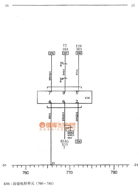
Sail anti-theft system circuit diagram shown as follow:
(View)
View full Circuit Diagram | Comments | Reading(1364)
Sail airbag system schematic
Published:2014/4/2 21:18:00 Author:lynne | Keyword: Sail airbag system schematic
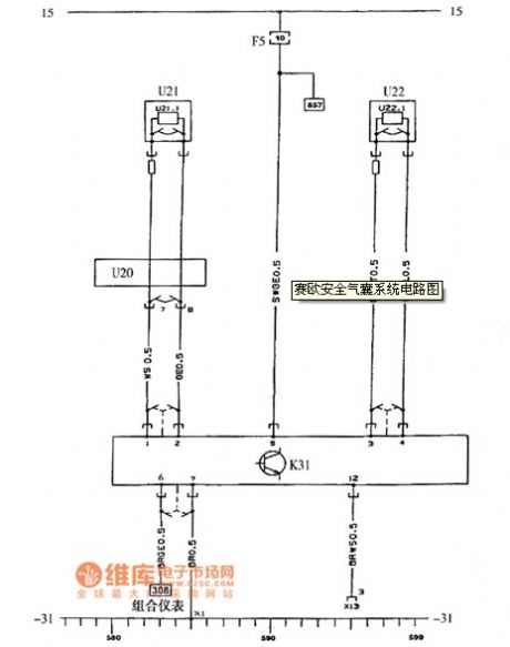
Sail airbag system schematic as shown:
(View)
View full Circuit Diagram | Comments | Reading(1443)
SF-10 module interface and temperature sensor circuit diagram
Published:2014/4/2 21:13:00 Author:lynne | Keyword: SF-10 module interface and temperature sensor circuit diagram
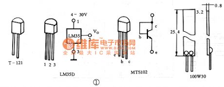
After the SF-10 Series Universal Control Module (Articles 1998 introduced the first one made) is available, a variety of upper and lower temperature controller design becomes very simple. In other words, just select the appropriate temperature sensor according to the control of the temperature range, according to the controlled object selection heater or cooling device, and then design temperature sensor and interface circuitry SF-10 on the line. This article describes some of the common temperature sensor interface circuit SF-10, and for the reader. Its shape and pin as shown.
(View)
View full Circuit Diagram | Comments | Reading(2970)
F-V conversion circuit schematic
Published:2014/4/2 21:12:00 Author:lynne | Keyword: F-V conversion circuit schematic

F-V conversion circuit schematic shown as follow:
(View)
View full Circuit Diagram | Comments | Reading(1714)
The LM35D interface circuit diagram
Published:2014/4/2 21:09:00 Author:lynne | Keyword: The LM35D interface circuit diagram,
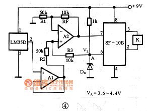
The interface circuit LM35D LM35D sensitivity of 10mV / ℃, it is up to 1V at 100 ℃ output. As the SF-10 instrument amplifier maximum input voltage of 240mV, so the higher the maximum temperature of the output signal LM35D to be attenuated. Further, LM35D voltage signal is output to ground, it can not directly access the output signal of the two inputs of the SF-10B (the ground pin ⑥, a single power amplifier device can not work), which requires the output voltage decays , and after the transfer circuit voltage to the interface with the SF-10B, as shown in FIG.
(View)
View full Circuit Diagram | Comments | Reading(1595)
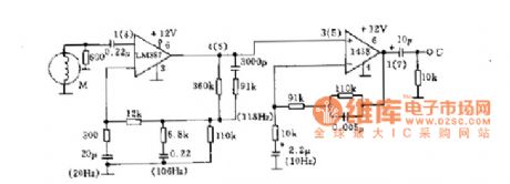
Telecom filter circuit schematic
Published:2014/4/2 21:20:00 Author:lynne | Keyword: Telecom filter circuit schematic
Telecom filter circuit schematic shown as follow:
(View)
View full Circuit Diagram | Comments | Reading(1510)
| Pages:9/2234 1234567891011121314151617181920Under 20 |
Circuit Categories
power supply circuit
Amplifier Circuit
Basic Circuit
LED and Light Circuit
Sensor Circuit
Signal Processing
Electrical Equipment Circuit
Control Circuit
Remote Control Circuit
A/D-D/A Converter Circuit
Audio Circuit
Measuring and Test Circuit
Communication Circuit
Computer-Related Circuit
555 Circuit
Automotive Circuit
Repairing Circuit