TISP3260F3, TISP3290, TISP3290L Selling Leads, Datasheet
MFG:PI Package Cooled:10000 D/C:06+

TISP3260F3, TISP3290, TISP3290L Datasheet download

Part Number: TISP3260F3
MFG: PI
Package Cooled: 10000
D/C: 06+


MFG:PI Package Cooled:10000 D/C:06+
TISP3260F3, TISP3290, TISP3290L Datasheet download
MFG: PI
Package Cooled: 10000
D/C: 06+

Want to post a buying lead? If you are not a member yet, please select the specific/related part number first and then fill the quantity and your contact details in the "Request for Quotation Form" on the left, and then click "Send RFQ".Your buying lead can then be posted, and the reliable suppliers will quote via our online message system or other channels soon.
TOP
PDF/DataSheet Download
Datasheet: TISP3260F3
File Size: 468729 KB
Manufacturer: POINN [Power Innovations Limited]
Download : Click here to Download
PDF/DataSheet Download
Datasheet: TISP3290
File Size: 113089 KB
Manufacturer: POINN [Power Innovations Limited]
Download : Click here to Download
PDF/DataSheet Download
Datasheet: TISP3290L
File Size: 115118 KB
Manufacturer: POINN [Power Innovations Limited]
Download : Click here to Download
These high voltage dual symmetrical transient voltage suppressor devices are designed to protect telecommunication applications with ground backed ringing against transients caused by lightning strikes and a.c. power lines. Offered in five voltage variants to meet battery and protection requirements they are guaranteed to suppress and withstand the listed international lightning surges in both polarities. Transients are initially clipped by breakdown clamping until the voltage rises to the breakover level, which causes the device to crowbar. The high crowbar holding current prevents d.c. latchup as the current subsides.
These monolithic protection devices are fabricated in ion-implanted planar structures toensure precise and matched breakover control and are virtually transparent to the system in normal operation
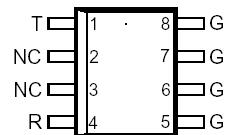
The small-outline 8 pin assignment has been carefully chosen for the TISP series to maximise the inter-pin clearance and creepage distances which are used by standards (e.g. IEC950) to establish voltage withstand ratings.
|
RATING |
SYMBOL |
VALUE |
UNIT | |
| Repetitive peak off-state voltage (0°C <TJ < 70°C) |
'3240F3 '3260F3 '3290F3 '3320F3 '3380F3 |
VDRM |
±180 ±200 ±220 ± 240 ± 270 |
V |
| Non-repetitive peak on-state pulse current (see Notes 1, 2 and 3) 1/2 µs (Gas tube differential transient, open-circuit voltage wave shape 1/2 µs) 2/10 µs (FCC Part 68, open-circuit voltage wave shape 2/10 µs) 8/20 µs (ANSI C62.41, open-circuit voltage wave shape 1.2/50 µs) 10/160 µs (FCC Part 68, open-circuit voltage wave shape 10/160 µs) 5/200 µs (VDE 0433, open-circuit voltage wave shape 2 kV, 10/700 µs) 0.2/310 µs (RLM 88, open-circuit voltage wave shape 1.5 kV, 0.5/700 µs) 5/310 µs (CCITT IX K17/K20, open-circuit voltage wave shape 2 kV, 10/700 µs) 5/310 µs (FTZ R12, open-circuit voltage wave shape 2 kV, 10/700 µs) 10/560 µs (FCC Part 68, open-circuit voltage wave shape 10/560 µs) 10/1000 µs (REA PE-60, open-circuit voltage wave shape 10/1000 µs) |
ITSP |
350 175 120 60 50 38 50 50 45 35 |
A | |
| Non-repetitive peak on-state current (see Notes 2 and 3) 50 Hz, 1 s |
D Package
P Package SL Package |
ITSM |
4
6 6 |
A rms |
| Initial rate of rise of on-state current, Linear current ramp, Maximum ramp value < 38 A |
diT/dt |
250 |
A/µs | |
| Junction temperature |
TJ |
-40 to +150 |
°C | |
| Storage temperature range |
Tstg |
-40 to +150 |
°C | |
The TISP3290 is designed specifically for telephone equipment protection against lightning and transients induced by a.c. power lines. These devices consist of two bidirectional suppressor elements connected to a Common (C) terminal. They will supress voltage transients between terminals A and C, B and C, and A and B.
Transients are initially clipped by zener action until the voltage rises to the breakover level, which causes the device to crowbar. The high crowbar holding current prevents d.c. latchup as the transient subsides.
These monolithic protection devices are fabricated in ion-implanted planar structures to ensure precise and matched breakover control and are virtually transparent to the system in normal operation.
|
RATING |
SYMBOL |
VALUE |
UNIT |
| Non-repetitive peak on-state pulse current (see Notes 1, 2 and 3) 8/20 µs (ANSI C62.41, open-circuit voltage wave shape 1.2/50 µs) 10/160 µs (FCC Part 68, open-circuit voltage wave shape 10/160 µs) 5/200 µs (VDE 0433, open-circuit voltage wave shape 2 kV, 10/700 µs) 0.2/310 µs (RLM 88, open-circuit voltage wave shape 1.5 kV, 0.5/700 µs) 5/310 µs (CCITT IX K17/K20, open-circuit voltage wave shape 2 kV, 10/700 µs) 5/310 µs (FTZ R12, open-circuit voltage wave shape 2 kV, 10/700 µs) 10/560 µs (FCC Part 68, open-circuit voltage wave shape 10/560 µs) 10/1000 µs (REA PE-60, open-circuit voltage wave shape 10/1000 µs) |
ITSP |
150 60 50 38 50 50 45 35 |
A |
| Non-repetitive peak on-state current, 50 Hz, 2.5 s (see Notes 1 and 2) |
ITSM |
10 |
A rms |
| Initial rate of rise of on-state current, Linear current ramp, Maximum ramp value < 38 A |
diT/dt |
250 |
A/µs |
| Junction temperature |
TJ |
150 |
°C |
| Operating free - air temperature range |
0 to 70 |
°C | |
| Storage temperature range |
Tstg |
-40 to +150 |
°C |
| Lead temperature 1.5 mm from case for 10 s |
Tlead |
260 |
°C |
The TISP3290L is designed specifically for telephone equipment protection against lightning and transients induced by a.c. power lines. These devices consist of two bidirectional suppressor elements connected to a Common (C) terminal. They will supress voltage transients between terminals A and C, B and C, and A and B.
Transients are initially clipped by zener action until the voltage rises to the breakover level, which causes the device to crowbar. The high crowbar holding current prevents d.c. latchup as the transient subsides.
These monolithic protection devices are fabricated in ion-implanted planar structures to ensure precise and matched breakover control and are virtually transparent to the system in normal operation.
|
RATING |
SYMBOL |
VALUE |
UNIT |
| Non-repetitive peak on-state pulse current (see Notes 1, 2 and 3) 8/20 µs (ANSI C62.41, open-circuit voltage wave shape 1.2/50 µs) 10/160 µs (FCC Part 68, open-circuit voltage wave shape 10/160 µs) 5/200 µs (VDE 0433, open-circuit voltage wave shape 2 kV, 10/700 µs) 0.2/310 µs (RLM 88, open-circuit voltage wave shape 1.5 kV, 0.5/700 µs) 5/310 µs (CCITT IX K17/K20, open-circuit voltage wave shape 2 kV, 10/700 µs) 5/310 µs (FTZ R12, open-circuit voltage wave shape 2 kV, 10/700 µs) 10/560 µs (FCC Part 68, open-circuit voltage wave shape 10/560 µs) 10/1000 µs (REA PE-60, open-circuit voltage wave shape 10/1000 µs) |
ITSP |
150 60 50 38 50 50 45 35 |
A |
| Non-repetitive peak on-state current, 50 Hz, 2.5 s (see Notes 1 and 2) |
ITSM |
10 |
A rms |
| Initial rate of rise of on-state current, Linear current ramp, Maximum ramp value < 38 A |
diT/dt |
250 |
A/µs |
| Junction temperature |
TJ |
150 |
°C |
| Operating free - air temperature range |
0 to 70 |
°C | |
| Storage temperature range |
Tstg |
-40 to +150 |
°C |
| Lead temperature 1.5 mm from case for 10 s |
Tlead |
260 |
°C |

Price: 4-6 USD
MT58L64L18CT-10 TQFP100

Price: 5-6.5 USD
DL-7140-211M laser tube

Price: 4-5 USD
74LVC74APG - IC FLIP FLOP D-Type POS-EDG DUAL 14TSSOP

Price: 6.5-8 USD
CYPRESS - Clock Synthesizer with Differential CPU Outputs

Price: 0.284-0.286 USD
PI5V330QEX Pericom Multiplexer Switch ICs

Price: 1-2 USD
IGBT power module, Single switch, 1200 V, Collector-emitter voltage, 430A

Price: 1-2 USD
a-Si TFT-LCD, NEC, 228.096Hmm, 560V

Price: 0.124-0.2 USD
PC354N1T - Mini-flat Package, AC Input Type Photocoupler - Sharp Electrionic Components

Price: 0.177-0.178 USD
RL1210JR51-XX-BL - Thick Film Chip Resistor Low Ohmic - TAITRON Components Incorporated

Price: 0.053-0.055 USD
STPS140A - POWER SCHOTTKY RECTIFIER - STMicroelectronics

Price: 1.45-1.5 USD
STA013 - MPEG 2.5 LAYER III AUDIO DECODER - STMicroelectronics

Price: 0.073-0.075 USD
SMBJ5347B - 5 Watt Surface Mount Silicon Zener Diodes - Micro Commercial Components
