TSA5523, TSA5523M, TSA5523M/C1 Selling Leads, Datasheet
MFG:PHILIPS Package Cooled:3230 D/C:01+

TSA5523, TSA5523M, TSA5523M/C1 Datasheet download

Part Number: TSA5523
MFG: PHILIPS
Package Cooled: 3230
D/C: 01+


MFG:PHILIPS Package Cooled:3230 D/C:01+
TSA5523, TSA5523M, TSA5523M/C1 Datasheet download
MFG: PHILIPS
Package Cooled: 3230
D/C: 01+

Want to post a buying lead? If you are not a member yet, please select the specific/related part number first and then fill the quantity and your contact details in the "Request for Quotation Form" on the left, and then click "Send RFQ".Your buying lead can then be posted, and the reliable suppliers will quote via our online message system or other channels soon.
TOP
PDF/DataSheet Download
Datasheet: TSA5523M
File Size: 186753 KB
Manufacturer: PHILIPS [Philips Semiconductors]
Download : Click here to Download
PDF/DataSheet Download
Datasheet: TSA5523M
File Size: 186753 KB
Manufacturer: PHILIPS [Philips Semiconductors]
Download : Click here to Download
PDF/DataSheet Download
Datasheet: TSA5523M/C1
File Size: 186753 KB
Manufacturer: PHILIPS [Philips Semiconductors]
Download : Click here to Download
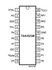
The device is a single chip PLL frequency synthesizer designed for TV and VCR tuning systems. The circuit consists of a divide-by-eight prescaler with its own preamplifier, a 15-bit programmable divider, a crystal oscillator and its programmable reference divider, a phase/frequency detector combined with a charge-pump which drives the tuning amplifier, including 33 V output. Three NPN open-collector outputs are provided for band switching together with five open-collector NPN outputs. Four of these ports can also be used as input ports (one ADC and three general purpose I/O ports).
An output is provided to control a Philips mixer/oscillator IC controlled by bits P7, P5 and P4. Depending on the reference divider ratio (512, 640 or 1024), the phase comparator operates at 3.90625, 6.25 or 7.8125 kHz with a 4 MHz crystal.
The lock detector bit FL is set to logic 1 when the loop is locked and is read on the SDA line (status byte) during a read operation. The ADC is available for digital AFC control. The ADC code is read during a read operation on the I2C-bus. The ADC input is combined with the port P6. In the test mode, this port is also used as a test output for fref and fdiv/2 (see Table 4). In addition, the circuit includes a DC/DC converter driver connected to the IDC pin to control the amplitude of an external oscillator followed by a voltage rectifier.
The voltage rectifier is used to generate the correct tuning supply voltage to maintain a constant current into the tuning amplifier. The DC/DC converter driver can be disabled by setting the IDC pin to VCC1 in this event the tuning supply voltage is delivered by a fixed 33 V supply. Five serial bytes (including address byte) are required to address the device, select the VCO frequency, program the ports, set the charge-pump current and set the reference divider ratio. The device has four independent I2C-bus addresses which can be selected by applying a specific voltage on the AS input (see Table 3).
| SYMBOL | PARAMETER | CONDITIONS | MIN. | MAX. | UNIT |
| ViRF | prescaler input voltage |
-0.3 | VCC1 | V | |
|
VCC1 |
supply voltage (+5 V) | -0.3 | +6 | V | |
| VoIDC | IDC output voltage | -0.3 | VCC1 | V | |
| VoNPN | NPN open-collector output voltage | -0.3 | +16 | V | |
| IoNPN | NPN open-collector output current | -1 | +15 | V | |
| VoCP | charge-pump output voltage | -0.3 | +Vcc1 | V | |
| Vo(tune) | tuning voltage output | see Fig.3 | -0.3 | +40 | V |
| VoBS | band-switch output voltage | -0.3 | Vcc1 | V | |
| ViSCL | serial clock input voltage | -0.3 | +6 | V | |
| Vi/oSDA | serial data input/output voltage | -0.3 | +6 | V | |
| IoSDA | data output current | -0.3 | +5 | V | |
| ViAS | address selection input voltage | -0.3 | +Vcc1 | mA | |
| ViXTAL | crystal input voltage | -0.3 | +Vcc1 | ||
| Tstg | IC storage temperature | -40 | +150 | ||
| tTj(max) | maximum junction temperature | - | +150 | s | |
| tsc | short-circuit time every pin to VCC1 or GND | - | 10 | s |

Price: 4-6 USD
MT58L64L18CT-10 TQFP100

Price: 5-6.5 USD
DL-7140-211M laser tube

Price: 4-5 USD
74LVC74APG - IC FLIP FLOP D-Type POS-EDG DUAL 14TSSOP

Price: 6.5-8 USD
CYPRESS - Clock Synthesizer with Differential CPU Outputs

Price: 0.284-0.286 USD
PI5V330QEX Pericom Multiplexer Switch ICs

Price: 1-2 USD
IGBT power module, Single switch, 1200 V, Collector-emitter voltage, 430A

Price: 1-2 USD
a-Si TFT-LCD, NEC, 228.096Hmm, 560V

Price: 0.124-0.2 USD
PC354N1T - Mini-flat Package, AC Input Type Photocoupler - Sharp Electrionic Components

Price: 0.177-0.178 USD
RL1210JR51-XX-BL - Thick Film Chip Resistor Low Ohmic - TAITRON Components Incorporated

Price: 0.053-0.055 USD
STPS140A - POWER SCHOTTKY RECTIFIER - STMicroelectronics

Price: 1.45-1.5 USD
STA013 - MPEG 2.5 LAYER III AUDIO DECODER - STMicroelectronics

Price: 0.073-0.075 USD
SMBJ5347B - 5 Watt Surface Mount Silicon Zener Diodes - Micro Commercial Components
