Want to post a buying lead? If you are not a member yet, please select the specific/related part number first and then fill the quantity and your contact details in the "Request for Quotation Form" on the left, and then click "Send RFQ".Your buying lead can then be posted, and the reliable suppliers will quote via our online message system or other channels soon.
The UC1852 provides a low-cost solution to active power-factor correction (PFC) for systems that would otherwise draw high peak current pulses from AC power lines. This circuit implements zero-current switched boost conversion, producing sinusoidal input currents with a minimum of external components, while keeping peak current substantially below that of fully-discontinuous converters.
The UC1852 provides controlled switch on-time to regulate the output bulk DC voltage, an off-time defined by the boost inductor, and a zero-current sensing circuit to reactivate the switch cycle. Even though switching frequency varies with both load and instantaneous line voltage, it can be maintained within a reasonable range to minimize noise generation.
While allowing higher peak switch currents than continuous PFCs such as the UC1854, this device offers less external circuitry and smaller inductors, yet better performance and easier line-noise filtering than discontinuous current PFCs with no sacrifice in complexity or cost. The ability to obtain a power factor in excess of 0.99 makes the UC1852 an optimum choice for low-cost applications in the 50 to 500 watt power range. Protection features of these devices include under-voltage lockout, output clamping, peak-current limiting, and maximum-frequency clamping.
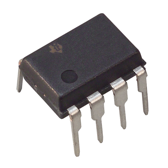
The UC1852 family is available in 8-pin plastic and ceramic dual in-line packages, and in the 8-pin small outline IC package (SOIC). The UC1852 is specified for operation from -55to +125, the UC2852 is specified for operation from -40 to +85, and the UC3852 is specified for operation from 0to +70.
UC2852 Maximum Ratings
Supply Voltage (Low-impedance Source)..........................30.0V Supply Current (High-impedance Source) ......................30.0mA OUT Current, Peak............................................................±1.0A OUT Energy, Capacitive Load............................................. 5.0J Input Voltage, ISNS ..........................................................±5.0V Input Voltage, VFB........................................... 0.3V to +10.0V COMP Current ..............................................................±10.0mA ISET Current.................................................................10.0mA Power Dissipation at Ta25 (Note 3) .............................1.0W Storage Temperature ........................................-65 to +150 Lead Temperature (Soldering, 10 Seconds) ................... +300
Note 1: All voltages with respect to GND (Pin 1). Note 2: All currents are positive into the specified terminal. Note 3: Refers to DIL-8 Package. Consult Packaging Section of Unitrode Integrated Circuits databook for thermal limitations and considerations of package.
UC2852 Features
· Low-Cost Power Factor Correction · Power Factor Greater Than 0.99 · Few External Parts Required · Controlled On-Time Boost PWM · Zero-Current Switching · Limited Peak Current · Min and Max Frequency Limits · Starting Current Less Than 1mA · High-Current FET Drive Output · Under-Voltage Lockout