W83176R-251, W83176R-733, W83176R-735 Selling Leads, Datasheet
MFG:SSOP Package Cooled:WINBOND D/C:0107+

W83176R-251, W83176R-733, W83176R-735 Datasheet download

Part Number: W83176R-251
MFG: SSOP
Package Cooled: WINBOND
D/C: 0107+


MFG:SSOP Package Cooled:WINBOND D/C:0107+
W83176R-251, W83176R-733, W83176R-735 Datasheet download
MFG: SSOP
Package Cooled: WINBOND
D/C: 0107+

Want to post a buying lead? If you are not a member yet, please select the specific/related part number first and then fill the quantity and your contact details in the "Request for Quotation Form" on the left, and then click "Send RFQ".Your buying lead can then be posted, and the reliable suppliers will quote via our online message system or other channels soon.
TOP
PDF/DataSheet Download
Datasheet: W83176G-732
File Size: 411857 KB
Manufacturer: WINBOND [Winbond]
Download : Click here to Download
PDF/DataSheet Download
Datasheet: W83176G-732
File Size: 411857 KB
Manufacturer: WINBOND [Winbond]
Download : Click here to Download
PDF/DataSheet Download
Datasheet: W83176R-735_06
File Size: 250935 KB
Manufacturer: WINBOND [Winbond]
Download : Click here to Download
The W83176R-733 is a 2.5V Dual Bank D.D.R. Clock buffer designed for VIA system. W83176R-733 can support 4 D.D.R. DRAM DIMMs.
The W83176R-733 provides I2C serial bus interface to program the registers to enable or disable each clock outputs. The W83176R-733 accepts a reference clock as its input and runs on 2.5V supply.
| PARAMETER | RATING |
| Voltage on any pin with respect to GND | - 0.5 V to + 3.6 V |
| Storage Temperature | - 65 to + 150 |
| Ambient Temperature | - 55 to + 125 |
| Operating Temperature | 0 to + 70 |
| Input ESD protection (Human body model) | 2000V |
These products are not designed for use in life support appliances, devices, or systems where malfunction of these products can reasonably be expected to result in personal injury. Winbond customers using or selling these products for use in such applications do so at their own risk and agree to fully indemnify Winbond for any damages resulting from such improper use or sales.
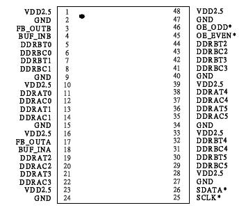
The W83176R-735 is a 2.5V Zero-delay D.D.R. Clock buffer designed for SiS system. W83176R-735 can support 3 D.D.R. DRAM DIMMs.
The W83176R-735 provides I2C serial bus interface to program the registers to enable or disable each clock outputs. The W83176R-735 accepts a reference clock as its input and runs on 2.5V supply.
| SYMBOL | PARAMETER | RATING |
| VDD, AVDD | Voltage on any pin with respect to GND | - 0.5 V to + 3.6 V |
| TSTG | Storage Temperature | - 65°C to + 150°C |
| TB | Ambient Temperature | - 55°C to + 125°C |
| TA | Operating Temperature | 0°C to + 70°C |


Price: 4-6 USD
MT58L64L18CT-10 TQFP100

Price: 5-6.5 USD
DL-7140-211M laser tube

Price: 4-5 USD
74LVC74APG - IC FLIP FLOP D-Type POS-EDG DUAL 14TSSOP

Price: 6.5-8 USD
CYPRESS - Clock Synthesizer with Differential CPU Outputs

Price: 0.284-0.286 USD
PI5V330QEX Pericom Multiplexer Switch ICs

Price: 1-2 USD
IGBT power module, Single switch, 1200 V, Collector-emitter voltage, 430A

Price: 1-2 USD
a-Si TFT-LCD, NEC, 228.096Hmm, 560V

Price: 0.124-0.2 USD
PC354N1T - Mini-flat Package, AC Input Type Photocoupler - Sharp Electrionic Components

Price: 0.177-0.178 USD
RL1210JR51-XX-BL - Thick Film Chip Resistor Low Ohmic - TAITRON Components Incorporated

Price: 0.053-0.055 USD
STPS140A - POWER SCHOTTKY RECTIFIER - STMicroelectronics

Price: 1.45-1.5 USD
STA013 - MPEG 2.5 LAYER III AUDIO DECODER - STMicroelectronics

Price: 0.073-0.075 USD
SMBJ5347B - 5 Watt Surface Mount Silicon Zener Diodes - Micro Commercial Components
