Want to post a buying lead? If you are not a member yet, please select the specific/related part number first and then fill the quantity and your contact details in the "Request for Quotation Form" on the left, and then click "Send RFQ".Your buying lead can then be posted, and the reliable suppliers will quote via our online message system or other channels soon.
General description of the BTS5240G are:(1)N channel vertical power MOSFET with charge pump, ground referenced CMOS compatible input and diagnostic feedback, monolithically integrated in Smart SIPMOS technology;(2)providing embedded protective functions;(3)extern adjustable current limitation.
The absolute maximum ratings of the BTS5240G can be summarized as:(1):the parameter is supply voltage,the symbol is Vbb,the values is 28,the unit is V;(2):the parameter is supply voltage for full short circuit protection Tj,start =-40 to +150,the symbol is Vbb,the values is 28,the unit is V;(3):the parameter is maximum voltage across DMOS,the symbol is VON,the values is 52,the unit is V;(4):the parameter is load dump protection VLoadDump = UA + Vs, UA = 13.5V RI = 2 , td = 400 ms; IN= low or high, RL = 2.25 RL = 6.8,the symbol is VLoad dump,the values is 40,53,the unit is V;(5):the parameter is operating temperature range,the symbol is Tj,the values is -40 to +150,the unit is ;(6):the parameter is storage temperature range,the symbol is Tstg,the values is -55 to +150,the unit is ;(7):the parameter is dynamical temperature rise at switching,the symbol is dT,the values is 60,the unit is K;(8):the parameter is power dissipation (DC) one channel active Ta = 85,the symbol is Ptot,the values is 1.4,the unit is W;(9):the parameter is continuous input voltage,the symbol is VIN,the values is -10 to 16,the unit is V;(10):the parameter is voltage at current limit adjustment pin,the symbol is VCLA,the values is -10 to 16,the unit is V;(11):the parameter is current limit adjustment current,the symbol is ICLA,the values is ±5.0,the unit is mA;(12):the parameter is current through input pin (DC),the symbol is IIN,the values is ±5.0,the unit is mA;(13):the parameter is current through sense (DC),the symbol is IIS,the values is -5 to 10,the unit is mA.
• N channel vertical power MOSFET with charge pump, ground referenced CMOS compatible input and diagnostic feedback, monolithically integrated in Smart SIPMOS® technology. • Providing embedded protective functions. • Extern adjustable current limitation.
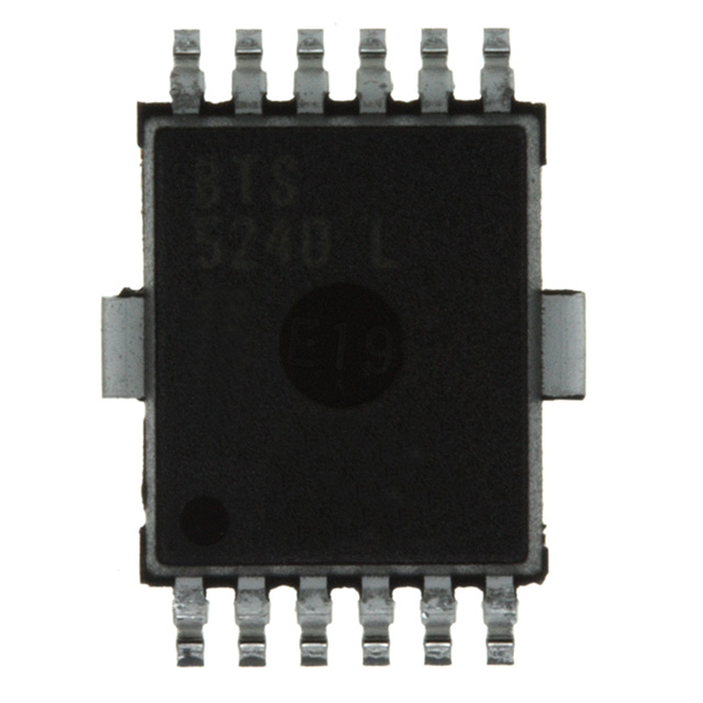
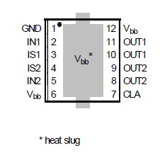
BTS5240L Maximum Ratings
Parameter
Symbol
Value
Unit
Supply voltage (overvoltage protection see page 6)
Vbb
281)
V
Supply voltage for full short circuit protection; Tj =-40 ...+150°C
Vbb(SC)
282)
Maximum voltage across DMOS
VON
52
Load dump protection3) VLoadDump4) = VA + VS; VA = 13,5 V In = low or high; td = 400 ms; RI4) = 2 RL = 2.25 RL = 6.8
VLoaddump
40 53
Load current (Short - circuit current, see page 7)
IL
IL(lim)5)
A
Operating temperature range
Tj
-40...+150
°C
Storage temperature range
Tstg
-55...+150
Dynamical temperature rise at switching
dT
60
K
Power dissipation6) (DC), one channel active TA = 85 °C
Ptot
1,4
W
Maximal switchable inductance, single pulse Vbb=12V, Tjstart=150°C; (see diagrams on page 12) IL = 6 A, EAS = 0.319 J, RL = 0 , one channel: IL = 12 A, EAS = 0.679 J, RL = 0 , two parallel channels:
ZL(s)
9.8 5.2
mH
Electrostatic discharge voltage IN: (Human Body Model) IS: according to ANSI EOS/ESD - S5.1 - 1993 , ESD STM5.1 - 1998 OUT:
VESD
1.0 2.0 4.0
kV
Continuous input voltage
VIN
-10...16
V
Voltage at current limit adjustment pin
VCLA
-10...16
Current limit adjustment current
ICLA
±5.0
mA
Current through input pin (DC)
IIN
±5.0
Current through sense (DC) (see page 11)
IIS
-5...10
BTS5240L Typical Application
• All types of resistive, inductive and capacitive loads • C compatible high-side power switch with diagnostic feedback for 12 V grounded loads • Due to the adjustable current limitation best suitable for loads with high inrush currents, so as lamps • Replaces electromechanical relays, fuses and discrete circuits