Want to post a buying lead? If you are not a member yet, please select the specific/related part number first and then fill the quantity and your contact details in the "Request for Quotation Form" on the left, and then click "Send RFQ".Your buying lead can then be posted, and the reliable suppliers will quote via our online message system or other channels soon.
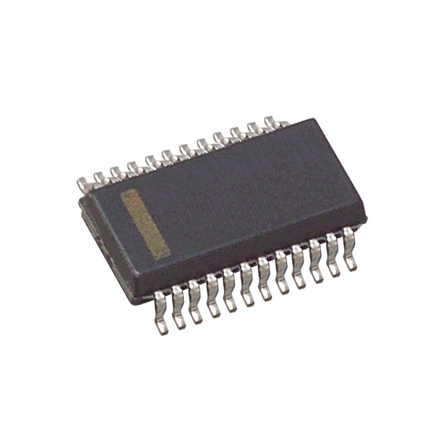
The CDC2351 is a high-performance clock-driver circuit that distributes one input (A) to ten outputs (Y) with minimum skew for clock distribution. The output-enable (OE) input disables the outputs to a high-impedance state. Each output has an internal series damping resistor to improve signal integrity at the load. The CDC2351 operates at nominal 3.3-V VCC. The propagation delays are adjusted at the factory using the P0 and P1 pins. The factory adjustments ensure that the part-to-part skew is minimized and is kept within a specified window. Pins P0 and P1 are not intended for customer use and should be connected to GND. The CDC2351 is characterized for operation from 0°C to 70°C.
† Stresses beyond those listed under "absolute maximum ratings" may cause permanent damage to the device. These are stress ratings only, and functional operation of the device at these or any other conditions beyond those indicated under "recommended operating conditions" is not implied. Exposure to absolute-maximum-rated conditions for extended periods may affect device reliability. NOTES: 1. The input and output negative-voltage ratings may be exceeded if the input and output clamp-current ratings are observed. 2. The maximum package power dissipation is calculated using a junction temperature of 150°C and a board trace length of 750 mils. For more information, refer to the Package Thermal Considerations application note in the 1994 ABT Advanced BiCMOS Technology Data Book, literature number SCBD002B.