CDC2510A

Features: Spread Spectrum Clock Compatible 100 MHz Maximum FrequencyAvailable in Plastic 24-Pin TSSOPPhase-Lock Loop Clock Distribution for Synchronous DRAM ApplicationsDistributes One Clock Input to One Bank of Five and One Bank of Four OutputsSeparate Output Enable for Each Output BankExternal F...

product image

CDC2510A Picture
SeekIC No. : 004312258 Detail

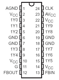
CDC2510A: Features: Spread Spectrum Clock Compatible 100 MHz Maximum FrequencyAvailable in Plastic 24-Pin TSSOPPhase-Lock Loop Clock Distribution for Synchronous DRAM ApplicationsDistributes One Clock Input t...

floor Price/Ceiling Price

Part Number:
CDC2510A
Supply Ability:
5000

Price Break

  • Qty
  • 1~5000
  • Unit Price
  • Negotiable
  • Processing time
  • 15 Days
Total Cost: $ 0.00

SeekIC Buyer Protection PLUS - newly updated for 2013!

  • Escrow Protection.
  • Guaranteed refunds.
  • Secure payments.
  • Learn more >>

Month Sales

268 Transactions

Rating

evaluate  (4.8 stars)

Upload time: 2024/5/1

Payment Methods

All payment methods are secure and covered by SeekIC Buyer Protection PLUS.

Notice: When you place an order, your payment is made to SeekIC and not to your seller. SeekIC only pays the seller after confirming you have received your order. We will also never share your payment details with your seller.
Product Details

Description


Features:

 Spread Spectrum Clock Compatible
100 MHz Maximum Frequency
 Available in Plastic 24-Pin TSSOP
 Phase-Lock Loop Clock Distribution for Synchronous DRAM Applications
 Distributes One Clock Input to One Bank of Five and One Bank of Four Outputs
 Separate Output Enable for Each Output Bank
 External Feedback (FBIN) Pin Is Used to Synchronize the Outputs to the Clock Input
 On-Chip Series Damping Resistors
 No External RC Network Required
 Operates at 3.3-V VCC


Pinout

  Connection Diagram


Specifications

Supply voltage , AVCC (see Note 1)  . . . . . . . . . . . . . . . . . . . . . . . . . . . . . .  .  . . . .  .AVCC < VCC +0.7 V
Supply voltage range, VCC, AVCC  . . . . . . . . . . . . . . . . . . . . . . . . . . . . . . . . . . . . . .. . .. .0.5 V to 4.6 V
Input voltage range, VI (see Note 2)  . . . . . . . . . . . . . . . . . . . . . . . . . . . . . . . . . . . . . . . .0.5 V to 6.5 V
Voltage range applied to any output in the high
or low state, VO (see Notes 2 and 3)  . . . . . . . . . . . . . . . . . . . . . . . . . . . . . . . . . . .0.5 V to VCC + 0.5 V
Input clamp current, IIK (VI < 0)  . . . . . . . . . . . . . . . . . . . . . . . . . . . . . . . . . . . . . . . . . . . . . . . . . .50 mA
Output clamp current, IOK (VO < 0 or VO > VCC) . . . . . . . . . . . . . . . . . . . . . . . . . . . . . . . . . . . . . .±50 mA
Continuous output current, IO (VO = 0 to VCC)  . . . . . . . . . . . . . . . . . . . . . . . . . . . . . . . . . . . . .. .±50 mA
Continuous current through each VCC or GND . . . . . . . . . . . . . . . . . . . . . . . . . . . . . . .. . . . . . . . ±100 mA
Maximum power dissipation at TA = 55°C (in still air) (see Note 4) . . . . . . . . . . . . . . . . .. . . . . . . . .0.7 W
Storage temperature range, Tstg . . . . . . . . . . . . . . . . . . . . . . . . . . . . . . . . . . . . . . . .. . . .65°C to 150°C


Description

The CDC2510A is a high-performance, low-skew, low-jitter, phase-lock loop (PLL) clock driver. It uses a PLL to precisely align, in both frequency and phase, the feedback (FBOUT) output to the clock (CLK) input signal. It is specifically designed for use with synchronous DRAMs. The CDC2510A operates at 3.3-V VCC and provides integrated series-damping resistors that make it ideal for driving point-to-point loads.

One bank of ten outputs CDC2510A provides ten low-skew, low-jitter copies of CLK. Output signal duty cycles are adjusted to 50 percent, independent of the duty cycle at CLK. All outputs can be enabled or disabled via a single output enable input. When the G input is high, the outputs switch in phase and frequency with CLK; when the G input is low, the outputs are disabled to the logic-low state.

Unlike many products containing PLLs, the CDC2510A does not require external RC networks. The loop filter for the PLL is included on-chip, minimizing component count, board space, and cost.

Because it is based on PLL circuitry, the CDC2510A requires a stabilization time to achieve phase lock of the feedback signal to the reference signal. This stabilization time is required, following power up and application of a fixed-frequency, fixed-phase signal at CLK, and following any changes to the PLL reference or feedback signals. The PLL can be bypassed for test purposes by strapping AVCC to ground.

The CDC2510A is characterized for operation from 0°C to 70°C.


Customers Who Bought This Item Also Bought

Margin,quality,low-cost products with low minimum orders. Secure your online payments with SeekIC Buyer Protection.
Soldering, Desoldering, Rework Products
Boxes, Enclosures, Racks
Resistors
Prototyping Products
DE1
Industrial Controls, Meters
Inductors, Coils, Chokes
View more