Want to post a buying lead? If you are not a member yet, please select the specific/related part number first and then fill the quantity and your contact details in the "Request for Quotation Form" on the left, and then click "Send RFQ".Your buying lead can then be posted, and the reliable suppliers will quote via our online message system or other channels soon.
This N-Channel MOSFET has been designed specifically for switching on the primary side in the isolated DC/DC converter application. Any application requiring a 150V MOSFETs with low on-resistance and fast switching will benefit.
These MOSFETs feature faster switching and lower gate charge than other MOSFETs with comparable RDS(ON) specifications.
The result is a MOSFET that is easy and safer to drive (even at very high frequencies), and DC/DC power supply designs with higher overall efficiency.
FDP2570 Maximum Ratings
Symbol
Parameter
Ratings
Units
VDSS
Drain-Source Voltage
150
V
VGSS
Gate-Source Voltage
± 20
V
ID
Drain Current Continuous (Note 1) Pulsed (Note 1)
22
A A
50
PD
Total Power Dissipation @ TC = 25 Derate above 25
93
W
0.63
W°/C
TJ, TSTG
Operating and Storage Junction Temperature Range
65 to +175
FDP2570 Features
* 22 A, 150 V. RDS(ON) = 80 m @ VGS = 10 V RDS(ON) = 90 m @ VGS = 6 V * Low gate charge (40nC typical) * Fast switching speed * High performance trench technology for extremely low RDS(ON) * 175°C maximum junction temperature rating
FDP2572 Parameters
Technical/Catalog Information
FDP2572
Vendor
Fairchild Semiconductor
Category
Discrete Semiconductor Products
Mounting Type
Through Hole
FET Polarity
N-Channel
Drain to Source Voltage (Vdss)
150V
Current - Continuous Drain (Id) @ 25° C
29A
Rds On (Max) @ Id, Vgs
54 mOhm @ 9A, 10V
Input Capacitance (Ciss) @ Vds
1770pF @ 25V
Power - Max
135W
Packaging
Tube
Gate Charge (Qg) @ Vgs
34nC @ 10V
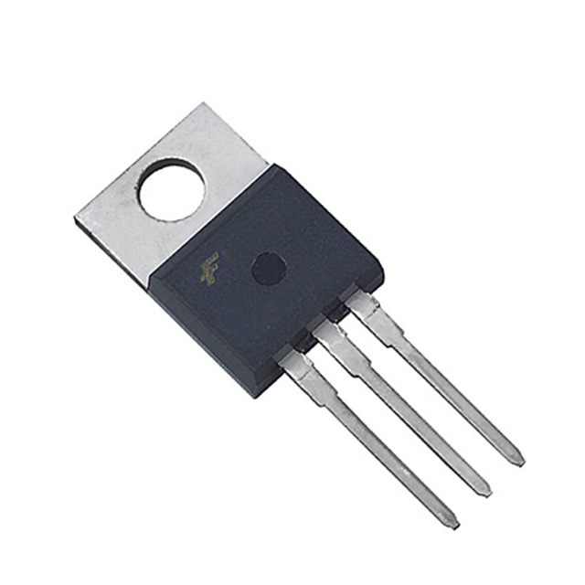
Package / Case
TO-220AB
FET Feature
Standard
Lead Free Status
Lead Free
RoHS Status
RoHS Compliant
Other Names
FDP2572 FDP2572
FDP2572 Maximum Ratings
Symbol
Parameter
Ratings
Units
VDSS
Drain-Source Voltage
150
V
VGSS
Gate-Source Voltage
±20
V
ID
Drain Current
Continuous (TC = 25, VGS = 10V)
29
A
Continuous (TC = 100, VGS = 10V)
20
A
Continuous (Tamb = 25, VGS = 10V, RJA = 43/W)
4
A
Pulsed
Figure 4
A
EAS
Single Pulse Avalanche Energy (Note 1)
36
mJ
PD
Power dissipation
135
W
Derate above 25
0.9
W/°C
TJ, Tstg
Operating and Storage Temperature
-55 to +175
°C
FDP2572 Features
• rDS(ON)= 45mΩ (Typ.), VGS = 10V, ID = 9A • Qg(tot) = 26nC (Typ.), VGS = 10V • Low Miller Charge • Low QRR Body Diode • UIS Capability (Single Pulse and Repetitive Pulse) • Qualified to AEC Q101
FDP2572 Typical Application
• DC/DC converters and Off-Line UPS • Distributed Power Architectures and VRMs • Primary Switch for 24V and 48V Systems • High Voltage Synchronous Rectifier • Direct Injection / Diesel Injection Systems • 42V Automotive Load Control • Electronic Valve Train Systems
FDP2670 Parameters
Technical/Catalog Information
FDP2670
Vendor
Fairchild Semiconductor
Category
Discrete Semiconductor Products
Mounting Type
Through Hole
FET Polarity
N-Channel
Drain to Source Voltage (Vdss)
200V
Current - Continuous Drain (Id) @ 25° C
19A
Rds On (Max) @ Id, Vgs
130 mOhm @ 10A, 10V
Input Capacitance (Ciss) @ Vds
1320pF @ 100V
Power - Max
93W
Packaging
Tube
Gate Charge (Qg) @ Vgs
38nC @ 10V
Package / Case
TO-220AB
FET Feature
Standard
Lead Free Status
Lead Free
RoHS Status
RoHS Compliant
Other Names
FDP2670 FDP2670
FDP2670 General Description
This N-Channel MOSFET has been designed specifically for switching on the primary side in the isolated DC/DC converter application. Any application requiring a 200V MOSFETs with low on-resistance and fast switching will benefit.
These MOSFETs feature faster switching and lower gate charge than other MOSFETs with comparable RDS(ON) specifications.
The result is a MOSFET that is easy and safer to drive (even at very high frequencies), and DC/DC power supply designs with higher overall efficiency.
FDP2670 Maximum Ratings
Symbol
Parameter
Ratings
Units
VDSS
Drain-Source Voltage
200
V
VGSS
Gate-Source Voltage
± 20
V
ID
Drain Current Continuous (Note 1) Pulsed (Note 1)
19
A A
40
PD
Total Power Dissipation @ TC = 25 Derate above 25
93
W
0.63
W°/C
dv/dt
Peak Diode Recovery dv/dt (Note 3)
3.2
V/ns
TJ, TSTG
Operating and Storage Junction Temperature Range
65 to +175
FDP2670 Features
* 19 A, 200 V. RDS(ON) = 130 m @ VGS = 10 V * Low gate charge (27 nC typical) * Fast switching speed * High performance trench technology for extremely low RDS(ON) * High power and current handling capability