Want to post a buying lead? If you are not a member yet, please select the specific/related part number first and then fill the quantity and your contact details in the "Request for Quotation Form" on the left, and then click "Send RFQ".Your buying lead can then be posted, and the reliable suppliers will quote via our online message system or other channels soon.
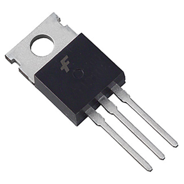
These N-Channel logic level enhancement mode power field effect transistors are produced using Fairchild's proprietary,high cell density, DMOS technology. This very high density process is especially tailored to minimize on-state resistance. These devices are particularly suited for low voltage applications such as DC/DC converters and high efficiency switching circuits where fast switching, low in-line power loss, and resistance to transients are needed.
FDP603AL Maximum Ratings
Symbol
Parameter
FDP603AL
FDB603AL
Units
VDSS
Drain-Source Voltage
30
V
VGSS
Gate-Source Voltage - Continuous
±20
V
ID
Drain Current - Continuous - Pulsed (Note 1)
33
A
100
PD
Total Power Dissipation @ TC = 25
50
W
Derate above 25
0.33
W/
TJ, TSTG
Operating and Storage Temperature Range
-65 to 175
TL
Maximum lead temperature for soldering purposes, 1/8" from case for 5 seconds
275
FDP603AL Features
*33 A, 30 V. RDS(ON) = 0.022 @ VGS =10 V RDS(ON) = 0.036 @ VGS =4.5 V. *Critical DC electrical parameters specified at elevated temperature. *Rugged internal source-drain diode can eliminate the need for an external Zener diode transient suppressor. *High density cell design for extremely low RDS(ON) . *175°C maximum junction temperature rating.
FDP61N20 Parameters
Technical/Catalog Information
FDP61N20
Vendor
Fairchild Semiconductor
Category
Discrete Semiconductor Products
Mounting Type
Through Hole
FET Polarity
N-Channel
Drain to Source Voltage (Vdss)
200V
Current - Continuous Drain (Id) @ 25° C
61A
Rds On (Max) @ Id, Vgs
41 mOhm @ 30.5A, 10V
Input Capacitance (Ciss) @ Vds
3380pF @ 25V
Power - Max
417W
Packaging
Tube
Gate Charge (Qg) @ Vgs
75nC @ 10V
Package / Case
TO-220
FET Feature
Standard
Drawing Number
*
Lead Free Status
Lead Free
RoHS Status
RoHS Compliant
Other Names
FDP61N20 FDP61N20
FDP61N20 General Description
These N-Channel enhancement mode power field effect transistors are produced using Fairchild's proprietary, planar stripe,DMOS technology.
This advanced technology has been especially tailored to minimize on-state resistance, provide superior switching performance, and withstand high energy pulse in the avalanche and commutation mode. These devices are well suited for high efficient switched mode power supplies and active power factor correction.
FDP61N20 Maximum Ratings
Symbol
Parameter
FDP61N20
Unit
VDSS
Drain-Source Voltage
200
V
ID
Drain Current - Continuous (TC= 25) - Continuous (TC= 100)
61 38.5
A A
IDM
Drain Current Pulsed (Note 1)
244
A
VGSS
Gate-Source voltage
±30
V
EAS
Single Pulsed Avalanche Energy (Note 2)
1440
mJ
IAR
I Avalanche Current (Note 1)
61
A
EAR
Repetitive Avalanche Energy (Note 1)
41.7
mJ
dv/dt
Peak Diode Recovery dv/dt (Note 3)
4.5
V/ns
PD
Power Dissipation (TC= 25) - Derate above 25
417 3.3
W W/
TJ,TSTG
Operating and Storage Temperature Range
-55to+150
TL
Maximum Lead Temperature for Soldering Purpose,1/8" from Case for 5 Seconds