Want to post a buying lead? If you are not a member yet, please select the specific/related part number first and then fill the quantity and your contact details in the "Request for Quotation Form" on the left, and then click "Send RFQ".Your buying lead can then be posted, and the reliable suppliers will quote via our online message system or other channels soon.
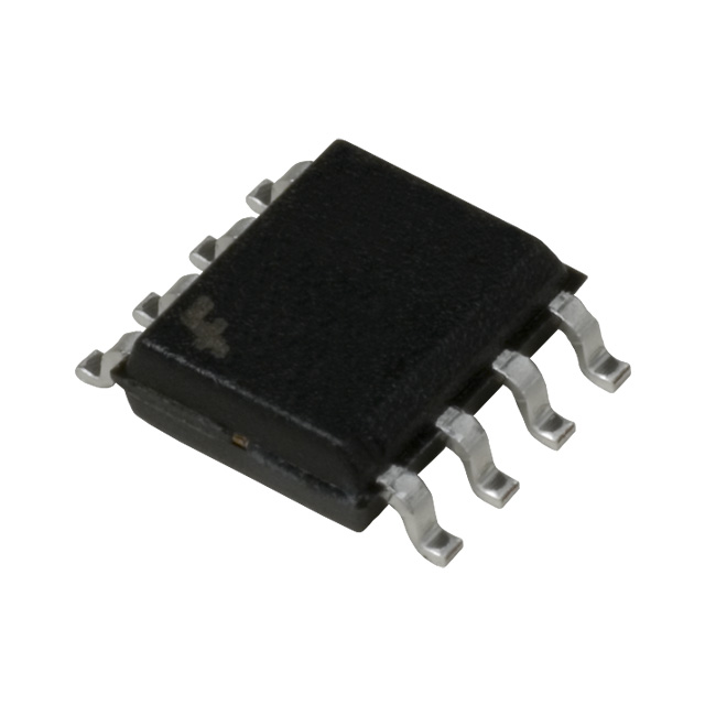
The FDS7064SN3 is designed to improve the efficiency of Buck Regulators. Used as the Synchronous rectifier, (Low side MOSFET), losses can be reduced, not only in this device, but also in the Control switch, (High side MOSFET). After the low side MOSFET turns off, reverse recovery current in the body diode is dissipated in the High Side device. A Discrete Schottky diode in parallel with the Low Side MOSFET can lower the reverse recovery current, but parasitic PCB and Package Inductance reduce the effectiveness of the Schottky. SyncFETTM technology reduces this inductance to a minimum by providing a monolithic solution (MOSFET and Schottky in the same die), resulting in optimum performance.
FDS7064SN3 Maximum Ratings
Symbol
Parameter
Ratings
Units
VDSS
Drain-Source Voltage
30
V
VGSS
Gate-Source Voltage
±16
V
ID
Drain Current - Continuous (Note 1a) - Pulsed
16
A
60
PD
Power Dissipation for Single Operation (Note 1a) (Note 1b)
3.13
W
1.5
TJ, TSTG
Operating and Storage Junction Temperature Range
-55to+150
°C
FDS7064SN3 Features
• 16 A, 30 V RDS(ON) = 8.0 mΩ @ VGS = 10 V RDS(ON) = 9.5 mΩ @ VGS = 4.5 V • High performance trench technology for extremely low RDS(ON) • No inductance between MOSFET and Schottky • 40% reduction in Body Diode Forward Voltage • Optimized to reduce losses in Synchronous Buck Regulators • FLMP SO-8 package for enhanced thermal performance.