Want to post a buying lead? If you are not a member yet, please select the specific/related part number first and then fill the quantity and your contact details in the "Request for Quotation Form" on the left, and then click "Send RFQ".Your buying lead can then be posted, and the reliable suppliers will quote via our online message system or other channels soon.
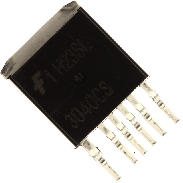
The FGB3040CS is an lgnition IGBT that offers outstanding SCIS capability along with a ratiometric emitter current sensing capability. This sensing is based on a emitter active area ratio of 200:1. The output is provided through a fourth (sense) lead. This signal provides a current level that is proportional to the main collector to emitter current. The effective ratio as measured on the sense lead is a function of the sense output, the collector current and the gate to emitter drive voltage.
FGB3040CS Maximum Ratings
Symbol
Parameter
Ratings
Units
BVCER
Collector to Emitter Breakdown Voltage (IC = 2mA)
430
V
BVECS
Emitter to Collector Breakdown Voltage (IC = 1mA) (Reverse Battery Condition)
24
V
ESCIS25
Self Clamping Inductive Switching Energy (at starting TJ = 25°C)
300
mJ
ESCIS150
Self Clamping Inductive Switching Energy (at starting TJ = 150°C)
170
mJ
IC25
Continuous Collector Current, at VGE = 4.0V, TC = 25°C
21
A
IC110
Continuous Collector Current, at VGE = 4.0V, TC = 110°C
19
A
PD
Maximum Continuous Gate to Emitter Voltage
±10
V
VGEM
Power Dissipation, at TC = 25°C
150
W
PD
Power Dissipation Derating, for TC > 25oC
1
W/
TJ
Operating Junction Temperature Range
-40 to 175
TSTG
Storage Junction Temperature Range
-40 to 175
TL
Max. Lead Temp. for Soldering (at 1.6mm from case for 10sec)
300
TPKG
Max. Package Temp. for Soldering (Package Body for 10 sec)
260
ESD
Electrostatic Discharge Voltage, HBM model (100pfd, 1500 ohms)
4
KV
FGB3040CS Features
·SCIS Energy = 300mJ at TJ = 25oC ·Logic Level Gate Drive
FGB30N6S2 General Description
The FGB30N6S2 is Low Gate Charge, Low Plateau Voltage SMPS II IGBTs combining the fast switching speed of the SMPS IGBTs along with lower gate charge and plateau voltage and avalanche capability (UIS). These LGC devices shorten delay times, and reduce the power requirement of the gate drive. These devices are specially designed for high voltage switched mode power supply applications where low conduction loss, fast switching times and UIS capability are essential.SMPS II LGC devices are widely used in the fields of Power Factor Correction (PFC) circuits,full bridge topologies,half bridge topologies,push-Pull circuits,uninterruptible power supplies and zero voltage and zero current switching circuits. Here you can get some information about the features. The 100kHz operation is at 390V, 14A.The 200kHZ operation is at 390V,9A.Besides,it has 600V switching SOA capability.The typical fall time is 90ns at TJ = 125oC.The low gate charge is 23 nC at VGE = 15V.The low plateau voltage is 6.5V typical.The UIS rated is 150mJ.What's more,it has low conduction loss. You have to understand the maximum ratings at TC= 25 if you want to purchase the product.The BVCES (Collector to Emitter Breakdown Voltage) is 600 V.The IC25 (Collector Current Continuous,TC = 25) is 45 A.The IC110 (Collector Current Continuous,TC = 110) is 20 A.The ICM (Collector Current Pulsed) is 108 A.The VGES (Gate to Emitter Voltage Continuous) is ±20 V.The VGEM (Gate to Emitter Voltage Pulsed) is ±30 V.The SSOA (Switching Safe Operating Area at TJ = 150) is 60A at 600V.The EAS (Pulsed Avalanche Energy, ICE = 20A, L = 1.3mH, VDD = 50V) is 150 mJ.The PD (Power Dissipation Total TC = 25°C) is 167 W.The Power Dissipation Derating is 1.33 W/ at TC > 25.The TJ (Operating Junction Temperature Range) is from -55 to 150 .The TSTG (Storage Junction Temperature Range) is from -55 to 150 . The following is about the electrical characteristics at TJ = 25.The Minimum BVCES (Collector to Emitter Breakdown Voltage) is 600 V at IC = 250A, VGE = 0.The Min BVECS (Emitter to Collector Breakdown Voltage) is 10 V and the Max. is 25 V at IC = 10mA, VGE = 0.The Max. ICES (Collector to Emitter Leakage Current) is 100 A at VCE = 600V,TJ = 25 and 2 mA at VCE = 600V,TJ = 125.The Max IGES (Gate to Emitter Leakage Current) is ±250 nA at VGE = ± 20V.The Typical VCE(SAT) (Collector to Emitter Saturation Voltage) is 2.0 V and the Max is 2.5V at IC = 12A,VGE = 15V,TJ = 25.The Typical VCE(SAT) (Collector to Emitter Saturation Voltage) is 1.7 V and the Max is 2.0 V at IC = 12A,VGE = 15V,TJ = 125.
FGB30N6S2 Maximum Ratings
FGB30N6S2 Features
FGB30N6S2D General Description
The FGH30N6S2D, FGP30N6S2D, and FGB30N6S2D are Low Gate Charge, Low Plateau Voltage SMPS II IGBTs combining the fast switching speed of the SMPS IGBTs along with lower gate charge and plateau voltage and ava-anche capability (UIS). These LGC devices shorten delay imes, and reduce the power requirement of the gate drive.
These devices are ideally suited for high voltage switched mode power supply applications where low conduction oss, fast switching times and UIS capability are essential.SMPS II LGC devices have been specially designed for:
FGB30N6S2D Maximum Ratings
Symbol
Parameter
Ratings
Units
BVCES
Collector to Emitter Breakdown Voltage
600
V
IC25
Collector Current Continuous, TC = 25°C
45
A
IC110
Collector Current Continuous, TC = 110°C
20
A
ICM
Collector Current Pulsed (Note 1)
108
A
VGES
Gate to Emitter Voltage Continuous
±20
V
VGEM
Gate to Emitter Voltage Pulsed
±30
V
SSOA
Switching Safe Operating Area at TJ = 150°C, Figure 2