Want to post a buying lead? If you are not a member yet, please select the specific/related part number first and then fill the quantity and your contact details in the "Request for Quotation Form" on the left, and then click "Send RFQ".Your buying lead can then be posted, and the reliable suppliers will quote via our online message system or other channels soon.
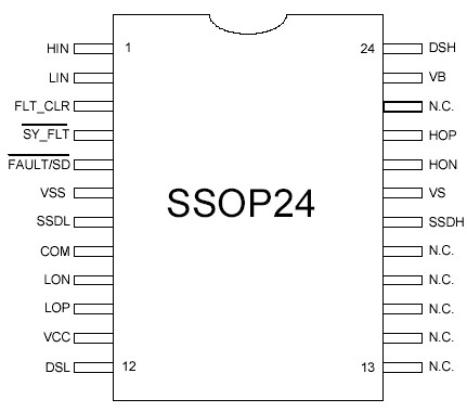
The IR2114/21141/2214/IR22141 gate driver family is suited to drive a single half bridge in power switching applications. The high gate driving capability (2A source, 3A sink) and the low quiescent current enable bootstrap supply techniques in medium power systems. These drivers feature full short circuit protection by means of the power transistor desaturation detection and manages all the half-bridge faults by turning off smoothly the desaturated transistor through the dedicated soft shut down pin, therefore preventing over-voltages and reducing EM emissions. In multi-phase system IR2114/21141/2214/IR22141 drivers communicate using a dedicated local network (SY_FLT and FAULT/SD signals) to properly manage phase-to-phase short circuits. The system controller may force shutdown or read device fault state through the 3.3 V compatible CMOS I/O pin (FAULT/SD). To improve the signal immunity from DC-bus noise, the control and power ground use dedicated pins enabling low-side emitter current sensing as well. Undervoltage conditions in floating and low voltage circuits are managed independently.
IR2114SS Maximum Ratings
Symbol
Definition
Min.
Max.
Units
VS
High side offset voltage
VB - 25
VB + 0.3
V
VB
High side floating supply voltage
(IR2114 or IR21141)
-0.3
625
(IR2214 or IR22141)
-0.3
1225
VHO
High side floating output voltage (HOP, HON and SSDH)
VS - 0.3
VB + 0.3
VCC
Low side and logic fixed supply voltage
-0.3
25
COM
Power ground
VCC - 25
VCC + 0.3
VLO
Low side output voltage (LOP, LON and SSDL)
VCOM -0.3
VCC + 0.3
VIN
Logic input voltage (HIN, LIN and FLT_CLR)
VSS -0.3
VCC + 0.3
VFLT
FAULT input/output voltage (FAULT/SD and SY_FLT)
VSS -0.3
VCC + 0.3
VDSH
High side DS input voltage
VS -3
VB + 0.3
VDSL
Low side DS input voltage
VCOM -3
VCC + 0.3
dVs/dt
Allowable offset voltage slew rate
-
50
V/ns
PD
Package power dissipation @ TA +25
-
1.5
W
RthJA
Thermal resistance, junction to ambient
-
65
/W
TJ
Junction temperature
-
125
TS
Storage temperature
-55
150
TL
Lead temperature (soldering, 10 seconds)
-
300
IR2114SS Features
• Floating channel up to +600 or +1200V • Soft over-current shutdown • Synchronization signal to synchronize shut down with the other phases • Integrated desaturation detection circuit • Two stage turn on output for di/dt control • Separate pull-up/pull-down output drive pins • Matched delay outputs • Under voltage lockout with hysteresis band