Want to post a buying lead? If you are not a member yet, please select the specific/related part number first and then fill the quantity and your contact details in the "Request for Quotation Form" on the left, and then click "Send RFQ".Your buying lead can then be posted, and the reliable suppliers will quote via our online message system or other channels soon.
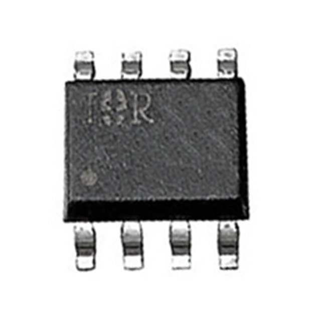
The IR2153D(S) are an improved version of the popular IR2155 and IR2151 gate driver ICs, and incorporates a high voltage half-bridge gate driver with a front end oscillator similar to the industry standard CMOS 555 timer. The IR2153 provides more functionality and is easier to use than previous ICs. A shutdown feature has been designed into the CT pin, so that both gate driver outputs can be disabled using a low voltage control signal. In addition, the gate driver output pulse widths are the same once the rising undervoltage lockout threshold on VCC has been reached, resulting in a more stable profile of frequency vs time at startup. Noise immunity has been improved significantly, both by lowering the peak di/dt of the gate drivers, and by increasing the undervoltage lockout hysteresis to 1V. Finally, special attention has been payed to maximizing the latch immunity of the device, and providing comprehensive ESD protection on all pins.
IR2153S Maximum Ratings
Symbol
Definition
Min.
Max.
Units
VB
High Side Floating Supply Voltage
-0.3
625
V
VS
High Side Floating Supply Offset Voltage
VB - 25
VB + 0.3
VHO
High Side Floating Output Voltage
VS - 0.3
VB + 0.3
VLO
Low Side Output Voltage
-0.3
VCC + 0.3
VRT
RT Voltage
-0.3
VCC + 0.3
VCT
CT Voltage
-0.3
VCC + 0.3
ICC
Supply Current (Note 1)
-
25
mA
IRT
RT Output Current
-5
5
dVs/dt
Allowable Offset Supply Voltage Transient
-
50
V/ns
PD
Package Power Dissipation @ TA +25°C
(8 Lead DIP)
-
1.0
W
(8 Lead SOIC)
-
0.625
RJA
Thermal Resistance, Junction to Ambient
(8 Lead DIP)
-
125
/W
(8 Lead SOIC)
-
200
TJ
Junction Temperature
-55
150
TS
Storage Temperature
-55
150
TL
Lead Temperature (Soldering, 10 seconds)
-
300
IR2153S Features
• Integrated 600V half-bridge gate driver • 15.6V zener clamp on Vcc • True micropower start up • Tighter initial deadtime control • Low temperature coefficient deadtime • Shutdown feature (1/6th Vcc) on CT pin • Increased undervoltage lockout Hysteresis (1V) • Lower power level-shifting circuit • Constant LO, HO pulse widths at startup • Lower di/dt gate driver for better noise immunity • Low side output in phase with RT • Internal 50nsec (typ.) bootstrap diode (IR2153D) • Excellent latch immunity on all inputs and outputs • ESD protection on all leads • Also available LEAD-FREE