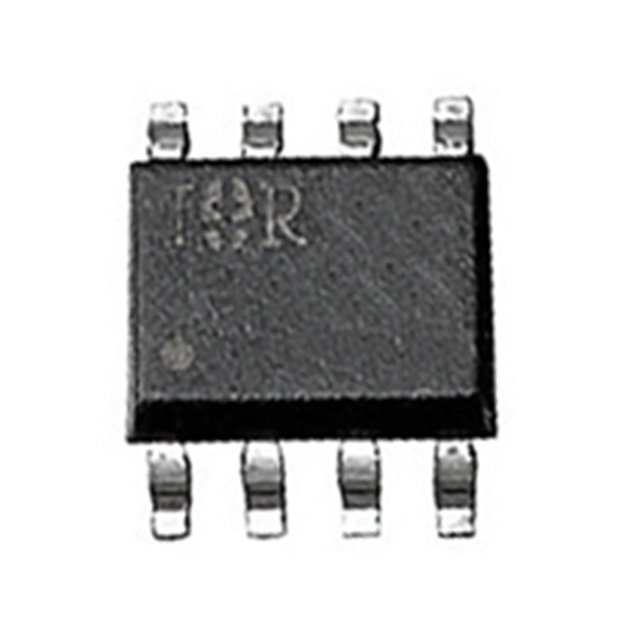
Want to post a buying lead? If you are not a member yet, please select the specific/related part number first and then fill the quantity and your contact details in the "Request for Quotation Form" on the left, and then click "Send RFQ".Your buying lead can then be posted, and the reliable suppliers will quote via our online message system or other channels soon.
The IR2184(4)(S) are high voltage, high speed power MOSFET and IGBT drivers with dependent high and low side referenced output channels. Proprietary HVIC and latch immune CMOS technologies enable ruggedized monolithic construction. The logic input is compatible with standard CMOS or LSTTL output, down to 3.3V logic. The output drivers feature a high pulse current buffer stage designed forminimum driver cross- conduction. The floating channel can be used to drive an N-channel power MOSFET or IGBT in the high side configuration which operates up to 600 volts.
IR2184 Maximum Ratings
Symbol
Definition
Min.
Max.
Units
VB
High side floating absolute voltage
-0.3
625
V
VS
High side floating supply offset voltage
VB - 25
VB + 0.3
VHO
High side floating output voltage
VS - 0.3
VB + 0.3
VCC
Low side and logic fixed supply voltage
-0.3
25
VLO
Low side output voltage
-0.3
VCC + 0.3
DT
Programmable dead-time pin voltage (IR21844 only)
VSS - 0.3
VCC + 0.3
VIN
Logic input voltage (IN & SD)
VSS - 0.3
VSS + 10
VSS
Logic ground (IR21844 only)
VCC - 25
VCC + 0.3
dVS/dt
Allowable offset supply voltage transient
-
50
V/ns
PD
Package power dissipation @ TA +25
(8 lead PDIP)
-
1.0
W
(8 lead SOIC)
-
0.625
(14 lead PDIP)
-
1.6
(14 lead SOIC)
-
1.0
RthJA
Thermal resistance, junction to ambient
(8 lead PDIP)
-
125
/W
(8 lead SOIC)
-
200
(14 lead PDIP)
-
75
(14 lead SOIC)
-
120
TJ
Junction temperature
-
150
TS
Storage temperature
-50
150
TL
Lead temperature (soldering, 10 seconds)
-
300
IR2184 Features
• Floating channel designed for bootstrap operation Fully operational to +600V Tolerant to negative transient voltage dV/dt immune • Gate drive supply range from 10 to 20V • Undervoltage lockout for both channels • 3.3V and 5V input logic compatible • Matched propagation delay for both channels • Logic and power ground +/- 5V offset. • Lower di/dt gate driver for better noise immunity • Output source/sink current capability 1.4A/1.8A
IR2184 Connection Diagram
IR21844 Parameters
Technical/Catalog Information
IR21844
Vendor
International Rectifier
Category
Integrated Circuits (ICs)
Configuration
Half Bridge
Voltage - Supply
10 V ~ 20 V
Current - Peak
1.9A
Delay Time
680ns
Package / Case
14-DIP (300 mil)
Packaging
Tube
Number of Outputs
2
Input Type
Non-Inverting
Number of Configurations
1
Operating Temperature
-40°C ~ 125°C
High Side Voltage - Max (Bootstrap)
600V
Lead Free Status
Contains Lead
RoHS Status
RoHS Non-Compliant
Other Names
IR21844 IR21844
IR21844 General Description
The IR2184(4)(S) are high voltage, high speed power MOSFET and IGBT drivers with dependent high and low side referenced output channels. Proprietary HVIC and latch immune CMOS technologies enable ruggedized monolithic construction. The logic input is compatible with standard CMOS or LSTTL output, down to 3.3V logic. The output drivers feature a high pulse current buffer stage designed forminimum driver cross- conduction. The floating channel can be used to drive an N-channel power MOSFET or IGBT in the high side configuration which operates up to 600 volts.
IR21844 Maximum Ratings
Symbol
Definition
Min.
Max.
Units
VB
High side floating absolute voltage
-0.3
625
V
VS
High side floating supply offset voltage
VB - 25
VB + 0.3
VHO
High side floating output voltage
VS - 0.3
VB + 0.3
VCC
Low side and logic fixed supply voltage
-0.3
25
VLO
Low side output voltage
-0.3
VCC + 0.3
DT
Programmable dead-time pin voltage (IR21844 only)
VSS - 0.3
VCC + 0.3
VIN
Logic input voltage (IN & SD)
VSS - 0.3
VSS + 10
VSS
Logic ground (IR21844 only)
VCC - 25
VCC + 0.3
dVS/dt
Allowable offset supply voltage transient
-
50
V/ns
PD
Package power dissipation @ TA +25
(8 lead PDIP)
-
1.0
W
(8 lead SOIC)
-
0.625
(14 lead PDIP)
-
1.6
(14 lead SOIC)
-
1.0
RthJA
Thermal resistance, junction to ambient
(8 lead PDIP)
-
125
/W
(8 lead SOIC)
-
200
(14 lead PDIP)
-
75
(14 lead SOIC)
-
120
TJ
Junction temperature
-
150
TS
Storage temperature
-50
150
TL
Lead temperature (soldering, 10 seconds)
-
300
IR21844 Features
• Floating channel designed for bootstrap operation Fully operational to +600V Tolerant to negative transient voltage dV/dt immune • Gate drive supply range from 10 to 20V • Undervoltage lockout for both channels • 3.3V and 5V input logic compatible • Matched propagation delay for both channels • Logic and power ground +/- 5V offset. • Lower di/dt gate driver for better noise immunity • Output source/sink current capability 1.4A/1.8A