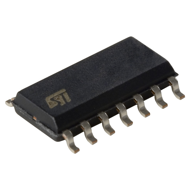
Want to post a buying lead? If you are not a member yet, please select the specific/related part number first and then fill the quantity and your contact details in the "Request for Quotation Form" on the left, and then click "Send RFQ".Your buying lead can then be posted, and the reliable suppliers will quote via our online message system or other channels soon.
This device is a monolithic quad Intelligent Power Switch in Multipower BCD Technology, for driving inductive, capacitive or resistive loads. Diagnostic for CPU feedback and extensive use of electrical protections make this device inherently indistructible and suitable for general purpose industrial applications.
L6376PD Maximum Ratings
Symbol
Pin
Parameter
Value
Unit
Vs
6
Supply Voltage (tw < 10ms)
50
V
Supply Voltage (DC)
40
V
Vs- Vout
Difference between supply voltage and output voltage
internally limited
Vid
16, 17
Externally Forced Voltage
-0.3 to 7
V
Iid
Externally Forced Current
±1
mA
Ii
12,13, 14,15, 18
Channel Input Current (forced)
±2
mA
Vi
Channel Input Voltage
-0.3 to 40
V
Iout
2, 3, 8, 9
Output Current (see also Isc)
internally limited
Vout
Output Voltage
internally limited
Eil
Energy Inductive Load (Tj =125°C); Each Channel
200
mJ
Ptot
Power Dissipation
internally limited
Vdiag
19
External voltage
-0.3 to Vs+0.7
V
Idiag
Externally forced current
-10 to 10
mA
Top
Ambient temperature, operating range
-25 to 85
°C
Tj
Junction temperature, operating range (see Overtemperature Protection)
-25 to 125
°C
Tstg
Storage temperature
-55 to 150
°C
L6376PD Connection Diagram
L6377 General Description
This device is a monolithic Intelligent Power Switch in Multipower BCD Technology for driving inductive, capacitive or resistive loads.
Diagnostic for CPU feedback and extensive use of electrical protections make this device inherently indistructible and suitable for general purpose industrial applications.
L6377 Maximum Ratings
Symbol
Pin
Parameter
Value
Unit
Vs
3
Supply Voltage (tw < 10ms)
50
V
Supply Voltage (DC)
40
V
Vs- Vout
3 vs 2
Supply to Output Differential voltage
internally limited
Vod
5
Externally Forced Voltage
-0.3 to 7
V
Iod
Externally Forced Current
±1
mA
IRESET
4
Reset Input Current (forced)
±2
mA
VRESET
Reset Input Voltage
-0.3 to 40
V
Iout
2
Output Current (see also Isc)
internally limited
Vout
Output Voltage
internally limited
Eil
Total Energy Inductive Load (Tj = 125°C)
50
mJ
Ptot
Power Dissipation
internally limited
Vdiag
6
External voltage
-0.3 to 40
V
Idiag
Externally forced current
-10 to 10
mA
Ii
7
Input Current
20
mA
Vi
Input Voltage
-10 to Vs +0.3
V
Top
Ambient temperature, operating range
-25 to 85
°C
Tj
Junction temperature, operating range (see Overtemperature Protection)
-25 to 125
°C
Tstg
Storage temperature
-55 to 150
°C
L6377 Connection Diagram
L6377D Parameters
Technical/Catalog Information
L6377D
Vendor
STMicroelectronics
Category
Integrated Circuits (ICs)
Package / Case
14-SOIC (3.9mm Width), 14-SOL
Mounting Type
Surface Mount
Type
High Side
Voltage - Supply
8 V ~ 35 V
On-State Resistance
-
Current - Output / Channel
500mA
Current - Peak Output
1.1A
Packaging
Tube
Input Type
Non-Inverting
Number of Outputs
1
Operating Temperature
-25°C ~ 85°C
Lead Free Status
Lead Free
RoHS Status
RoHS Compliant
Other Names
L6377D L6377D 497 1434 5 ND 49714345ND 497-1434-5
L6377D General Description
This device is a monolithic Intelligent Power Switch in Multipower BCD Technology for driving inductive, capacitive or resistive loads.
Diagnostic for CPU feedback and extensive use of electrical protections make this device inherently indistructible and suitable for general purpose industrial applications.
L6377D Maximum Ratings
Symbol
Pin
Parameter
Value
Unit
Vs
3
Supply Voltage (tw < 10ms)
50
V
Supply Voltage (DC)
40
V
Vs- Vout
3 vs 2
Supply to Output Differential voltage
internally limited
Vod
5
Externally Forced Voltage
-0.3 to 7
V
Iod
Externally Forced Current
±1
mA
IRESET
4
Reset Input Current (forced)
±2
mA
VRESET
Reset Input Voltage
-0.3 to 40
V
Iout
2
Output Current (see also Isc)
internally limited
Vout
Output Voltage
internally limited
Eil
Total Energy Inductive Load (Tj = 125°C)
50
mJ
Ptot
Power Dissipation
internally limited
Vdiag
6
External voltage
-0.3 to 40
V
Idiag
Externally forced current
-10 to 10
mA
Ii
7
Input Current
20
mA
Vi
Input Voltage
-10 to Vs +0.3
V
Top
Ambient temperature, operating range
-25 to 85
°C
Tj
Junction temperature, operating range (see Overtemperature Protection)