Want to post a buying lead? If you are not a member yet, please select the specific/related part number first and then fill the quantity and your contact details in the "Request for Quotation Form" on the left, and then click "Send RFQ".Your buying lead can then be posted, and the reliable suppliers will quote via our online message system or other channels soon.
The TLE202x, TLE202xA, and TLE202xB devices are precision, high-speed, low-power operational amplifiers using a new Texas Instruments Excalibur process. These devices combine the best features of the OP21 with highly improved slew rate and unity-gain bandwidth.
The complementary bipolar Excalibur process utilizes isolated vertical pnp transistors that yield dramatic improvement in unity-gain bandwidth and slew rate over similar devices.
The addition of a bias circuit in conjunction with this process results in extremely stable parameters with both time and temperature. This means that a precision device remains a precision device even with changes in temperature and over years of use.
This combination of excellent dc performance with a common-mode input voltage range that includes the negative rail makes these devices the ideal choice for low-level signal conditioning applications in either single-supply or split-supply configurations. In addition, these devices offer phase-reversal protection circuitry that eliminates an unexpected change in output states when one of the inputs goes below the negative supply rail.
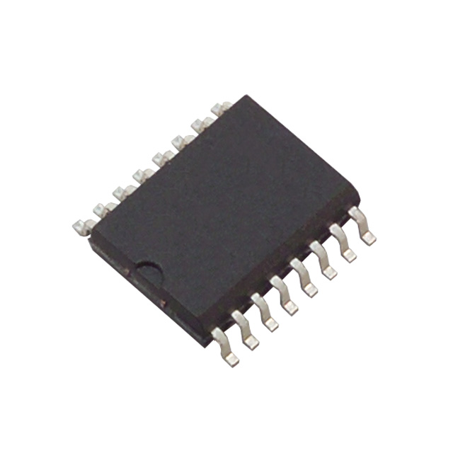
A variety of available options includes small-outline and chip-carrier versions for high-density systems applications.
The C-suffix devices are characterized for operation from 0°C to 70°C. The I-suffix devices are characterized for operation from 40°C to 85°C. The M-suffix devices are characterized for operation over the full military temperature range of 55°C to 125°C.
TLE2024 Maximum Ratings
Supply voltage, VCC+ (see Note 1) . . . . . . . . . . . . . . . . . . . . . . . . . . . . . . . . .. . .. . .. . . . . 20 V Supply voltage, VCC (see Note 1) . . . . . . . . . . . . . . . . . . . . . . . . . . . . .. . .. . .. . . . . . . . 20 V Differential input voltage, VID (see Note 2) . . . . . . . . . . . . . . . . . . . . . . . .. . .. . .. . . . . . . ±0.6 V Input voltage range, VI (any input, see Note 1) . . . . . . . . . . . . . . . . . . . .. . .. . .. . . . . . . . ±VCC Input current, II (each input) . . . . . . . . . . . . . . . . . . . . . . . . . . . . . . . . . . . . . . .. . .. . . . . ±1 mA Output current, IO (each output): TLE2021 . . . . . . . . . . . . . . . . . . . . . . . . . . . .. . . . . . . ±20 mA TLE2022 . . . . . . . . . . . . . . . . . . . . . . . . . . . . . . .. . . . ±30 mA TLE2024 . . . . . . . . . . . . . . . . . . . . . . . . . . . .. . . . . .. ±40 mA Total current into VCC+ . . . . . . . . . . . . . . . . . . . . . . . . . . . . . . . . . . . . . . . . . . .. . .. . . . . . 80 mA Total current out of VCC . . . . . . . . . . . . . . . . . . . . . . . . . . . . . . . . . . . . . . . . . .. . . . . . . . 80 mA Duration of short-circuit current at (or below) 25°C (see Note 3) . . . . . . . . . .. . .. . . . unlimited Continuous total power dissipation . . . . . . . . . . . . . . . . . . . . . . ... See Dissipation Rating Table Operating free-air temperature range, TA: C suffix . . . . . . . . . . . . . . . . . . . . . . . . .0°C to 70°C I suffix . . . . . . . . . . . . . . . . . . . . .. . .40°C to 85°C M suffix . . . . . . . . . . . . . . . . . . . . . .55°C to 125°C Storage temperature range, Tstg . . . . . . . . . . . . . . . . . . . . . . . . . . . . . . . . . .. . .65°C to 150°C Case temperature for 60 seconds, TC: FK package . . . . . . . . . . . . . . . . . . . . . . . . .. . .. . .260°C Lead temperature 1,6 mm (1/16 inch) from case for 10 seconds: D, DP, P, or PW package.260°C Lead temperature 1,6 mm (1/16 inch) from case for 60 seconds: JG package . . .. . .. . .. . .300°C † Stresses beyond those listed under "absolute maximum ratings" may cause permanent damage to the device. These are stress ratings only, and functional operation of the device at these or any other conditions beyond those indicated under "recommended operating conditions" is not implied. Exposure to absolute-maximum-rated conditions for extended periods may affect device reliability. NOTES: 1. All voltage values, except differential voltages, are with respect to the midpoint between VCC+, and VCC. 2. Differential voltages are at IN+ with respect to IN. Excessive current flows if a differential input voltage in excess of approximately ±600 mV is applied between the inputs unless some limiting resistance is used. 3. The output may be shorted to either supply. Temperature and/or supply voltages must be limited to ensure that the maximum dissipation rating is not exceeded.