Want to post a buying lead? If you are not a member yet, please select the specific/related part number first and then fill the quantity and your contact details in the "Request for Quotation Form" on the left, and then click "Send RFQ".Your buying lead can then be posted, and the reliable suppliers will quote via our online message system or other channels soon.
The TLK2201 and TLK2201I gigabit ethernet transceivers provide for ultrahigh-speed full-duplex point-to-point data transmissions. These devices are based on the timing requirements of the 10-bit interface specification by the IEEE 802.3 Gigabit Ethernet specification. The TLK2201 supports data rates from 1.0 Gbps through 1.6 Gbps and the TLK2201I supports data rates from 1.2 Gbps through 1.6 Gbps.
The primary application of these devices is to provide building blocks for point-to-point baseband data transmission over controlled impedance media of 50 or 75 . The transmission media can be printed-circuit board traces, copper cables or fiber-optical media. The ultimate rate and distance of data transfer is dependent upon the attenuation characteristics of the media and the noise coupling to the environment.
The TLK2201 and TLK2201I perform the data serialization, deserialization, and clock extraction functions for a physical layer interface device. The transceiver operates at 1.25 Gbps (typical), providing up to 1 Gbps of data bandwidth over a copper or optical media interface.
The TLK2201 and TLK2201I support both the defined 10-bit interface (TBI) and a reduced 5-bit interface utilizing double data rate (DDR) clocking. In the TBI mode the serializer/deserializer (SERDES) accepts 10-bit wide 8b/10b parallel encoded data bytes. The parallel data bytes are serialized and transmitted differentially at PECL compatible voltage levels. The SERDES extracts clock information from the input serial stream and deserializes the data, outputting a parallel 10-bit data byte.
In the DDR mode the parallel interface accepts 5-bit wide 8b/10b encoded data aligned to both the rising and falling edge of the reference clock. The data is clocked most significant bit first, (bits 0 4 of the 8b/10b encoded data) on the rising edge of the clock and the least significant bits (bits 5 9 of the 8b/10b encoded data) are clocked on the falling edge of the clock.
The TLK2201 and TLK2201I provide a comprehensive series of built-in tests for self-test purposes including loopback and pseudorandom binary sequence (PRBS) generation and verification. An IEEE 1149.1 JTAG port is also supported.
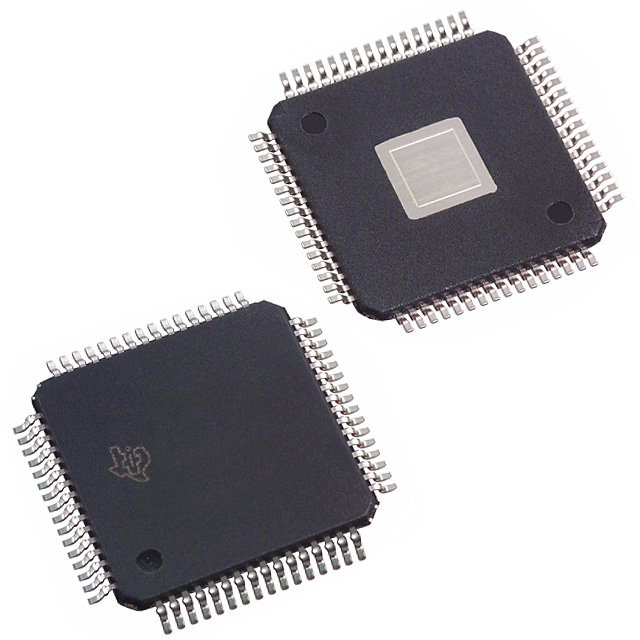
The TLK2201 and TLK2201I are housed in a high performance, thermally enhanced, 64-pin VQFP PowerPAD package. Use of the PowerPAD package does not require any special considerations except to note that the PowerPAD, which is an exposed die pad on the bottom of the device, is a metallic thermal and electrical conductor. It is recommended that the TLK2201 and TLK2201I PowerPADs be soldered to the thermal land on the board.
The TLK2201 is characterized for operation from 0°C to 70°C. The TLK2201I is characterized for operation from 40°C to 85°C.
The TLK2201 and TLK2201I use a 2.5-V supply. The I/O section is 3.3-V compatible. With the 2.5-V supply the chipset is very power-efficient, dissipating less than 200 mW typical power when operating at 1.25 Gbps.
The TLK2201 and TLK2201I are designed to be hot plug capable. A power-on reset causes RBC0, RBC1, the parallel output signal terminals, TXP, and TXN to be held in high-impedance state.
† Stresses beyond those listed under "absolute maximum ratings" may cause permanent damage to the device. These are stress ratings only, and functional operation of the device at these or any other conditions beyond those indicated under "recommended operating conditions" is not implied. Exposure to absolute-maximum-rated conditions for extended periods may affect device reliability.
TLK2201 Features
1 to 1.6 Gigabits Per Second (Gbps) Serializer/Deserializer (TLK2201) 1.2 to 1.6 Gigabits Per Second (Gbps) Serializer/Deserializer (TLK2201I) Low Power Consumption <200 mW at 1.25 Gbps LVPECL Compatible Differential I/O on High Speed Interface Single Monolithic PLL Design Support For 10 Bit Interface or Reduced Interface 5 Bit DDR (Double Data Rate) Clocking Receiver Differential Input Thresholds 200 mV Minimum Industrial Temperature Range From 40°C to 85°C (TLK2201I) IEEE 802.3 Gigabit Ethernet Compliant Advanced 0.25 m CMOS Technology No External Filter Capacitors Required Comprehensive Suite of Built-In Testability IEEE 1149.1 JTAG Support 2.5-V Supply Voltage for Lowest Power Operation 3.3-V Tolerant on LVTTL Inputs Hot Plug Protection 64-Pin VQFP With Thermally Enhanced Package (PowerPAD)
TLK2201 Connection Diagram
TLK2201A General Description
The TLK2201A and TLK2201AI gigabit ethernet transceivers provide for ultrahigh-speed full-duplex point-to-point data transmissions. These devices are based on the timing requirements of the 10-bit interface specification by the IEEE 802.3 Gigabit Ethernet specification. The TLK2201A supports data rates from 1.0 Gbps through 1.6 Gbps and the TLK2201AI supports data rates from 1.2 Gbps through 1.6 Gbps.
The primary application of these devices is to provide building blocks for point-to-point baseband data transmission over controlled impedance media of 50 or 75 . The transmission media can be printed circuit board traces, copper cables or fiber-optical media. The ultimate rate and distance of data transfer is dependent upon the attenuation characteristics of the media and the noise coupling to the environment. The TLK2201A and TLK2201AI perform the data serialization, deserialization, and clock extraction functions for a physical layer interface device. The transceiver operates at 1.25 Gbps (typical), providing up to 1 Gbps of data bandwidth over a copper or optical media interface.
The TLK2201A and TLK2201AI support both the defined 10-bit interface (TBI) and a reduced 5-bit interface utilizing double data rate (DDR) clocking. In the TBI mode the serializer/deserializer (SERDES) accepts 10-bit wide 8b/10b parallel encoded data bytes. The parallel data bytes are serialized and transmitted differentially at PECL compatible voltage levels. The SERDES extracts clock information from the input serial stream and deserializes the data, outputting a parallel 10-bit data byte.
In the DDR mode the parallel interface accepts 5-bit wide 8b/10b encoded data aligned to both the rising and falling edge of the reference clock. The data is clocked most significant bit first, (bits 0 4 of the 8b/10b encoded data) on the rising edge of the clock and the least significant bits (bits 5 9 of the 8b/10b encoded data) are clocked on the falling edge of the clock.
The TLK2201A and TLK2201AI provide a comprehensive series of built-in tests for self-test purposes including loopback and pseudorandom binary sequence (PRBS) generation and verification. An IEEE 1149.1 JTAG port is also supported.
The TLK2201A and TLK2201AI are housed in a high performance, thermally enhanced, 64-pin VQFP PowerPAD package. Use of the PowerPAD package does not require any special considerations except to note that the PowerPAD, which is an exposed die pad on the bottom of the device, is a metallic thermal and electrical conductor. It is recommended that the TLK2201A and TLK2201AI PowerPADs be soldered to the thermal land on the board.
The TLK2201A is characterized for operation from 0°C to 70°C. The TLK2201AI is characterized for operation from 40°C to 85°C.
The TLK2201A and TLK2201AI use a 2.5-V supply. The I/O section is 3.3-V compatible. With the 2.5-V supply the chipset is very power-efficient, dissipating less than 200 mW typical power when operating at 1.25 Gbps.
The TLK2201A and TLK2201AI are designed to be hot plug capable. A power-on reset causes RBC0, RBC1, the parallel output signal terminals, TXP, and TXN to be held in high-impedance state.
TLK2201A Maximum Ratings
Supply voltage, VDD (see Note 1) . . . . . . . . . . . . . . . . . . . . . . . . . . . . . . . . . . . . . . . . . . . . . 0.3 V to 3 V Input voltage range at TTL terminals, VI . . . . . . . . . . . . . . . . . . . . . . . . . . . . . . . . . . . . . . . . 0.5 V to 4 V Input voltage range at any other terminal . . . . . . . . . . . . . . . . . . . . . . . . . . . . . . . . 0.3 V to VDD +0.3 V Storage temperature, Tstg . . . . . . . . . . . . . . . . . . . . . . . . . . . . . . . . . . . . . . . . . . . . . . 65°C to 150°C Electrostatic discharge . . . . . . . . . . . . . . . . . . . . . . . . . . . . . . . . . . . . . . . . . . . . . . . CDM: 1 kV, HBM:2 kV Characterized free-air operating temperature range . . . . . . . . . . . . . . . . . . . . . . . . . . . . . . . 0°C to 70° Characterized free-air operating temperature range: TLK2201A . . . . . . . . . . . . . . . . . . . . 0°C to 70°C TLK2201AI . . . . . . . . . . . . . . . . . . 40°C to 85°C † Stresses beyond those listed under "absolute maximum ratings" may cause permanent damage to the device. These are stress ratings only, and functional operation of the device at these or any other conditions beyond those indicated under "recommended operating conditions" is not implied. Exposure to absolute-maximum-rated conditions for extended periods may affect device reliability. NOTE 1: All voltage values, except differential I/O bus voltages, are with respect to network ground terminal.
TLK2201A Features
1 to 1.6 Gigabits Per Second (Gbps) Serializer/Deserializer (TLK2201A) 1.2 to 1.6 Gigabits Per Second (Gbps) Serializer/Deserializer (TLK2201AI) Low Power Consumption <200 mW at 1.25 Gbps LVPECL Compatible Differential I/O on High Speed Interface Single Monolithic PLL Design Support For 10 Bit Interface or Reduced Interface 5 Bit DDR (Double Data Rate) Clocking Receiver Differential Input Thresholds 200 mV Minimum Industrial Temperature Range From 40°C to 85°C (TLK2201AI) IEEE 802.3 Gigabit Ethernet Compliant Advanced 0.25 m CMOS Technology No External Filter Capacitors Required Comprehensive Suite of Built-In Testability IEEE 1149.1 JTAG Support 2.5-V Supply Voltage for Lowest Power Operation 3.3-V Tolerant on LVTTL Inputs Hot Plug Protection 64-Pin VQFP With Thermally Enhanced Package (PowerPAD™)