Position: Home > DataSheet > Index V > VNS Series > VNS1NV04D, VNS3NV04, VNS3NV04D
Low Cost Custom Prototype PCB Manufacturer

VNS1NV04D, VNS3NV04, VNS3NV04D

VNS1NV04D, VNS3NV04, VNS3NV04D Selling Leads, Datasheet

MFG:STMicroelectronics  Category:Integrated Circuits (ICs)  Package Cooled:ex-stcok  D/C:03+

VNS1NV04D Picture

VNS1NV04D, VNS3NV04, VNS3NV04D Datasheet download

Five Points

Part Number: VNS1NV04D

Category: Integrated Circuits (ICs)

MFG: STMicroelectronics

Package Cooled: ex-stcok

D/C: 03+

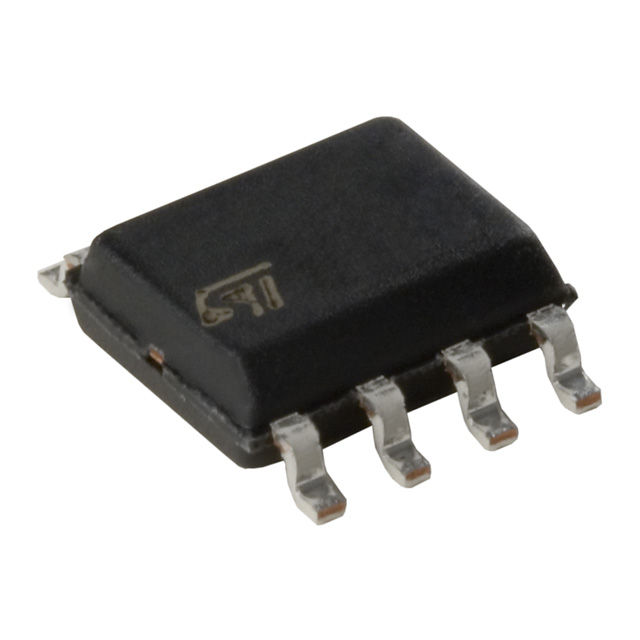
Description: MOSFET 2N-CH 40V 3.5A 8-SOIC

Price Break

2000

Unit Price

.67095

Extended Price

1341.90

(All prices are in USD) Prices for reference only
Urgent Purchase
Attentive hint

Want to post a buying lead? If you are not a member yet, please select the specific/related part number first and then fill the quantity and your contact details in the "Request for Quotation Form" on the left, and then click "Send RFQ".Your buying lead can then be posted, and the reliable suppliers will quote via our online message system or other channels soon.


Top Sellers:

TOP

VNS1NV04D Suppliers

More VNS1NV04D Suppliers

Select All  

  • VNS1NV04D

  • Vendor: STM Pack: Original D/C: 12+& Qty: 2000000  Adddate: 2024-04-28
  • Inquire Now
  • TODENKI ELECTRONICS COMPANY   China
    Contact: Ms.Alice  
    Tel: 86-755-82565937
    Fax: 86-755-83206987
    (14)
  • VNS14Q575-FC

  • D/C: 07+&   Adddate: 2024-04-28
  • Inquire Now
  • Guangzheng tech   China
    Contact: Ms.landy lu   MSN:gz-tech2@hotmail.com
    Tel: 0086-0755-83666664
    Fax: 0086-0755-83681577
    (0)
  • VNS1NV04D

  • Vendor: STM Pack: Original D/C: 12+& Qty: 2000000  Adddate: 2024-04-28
  • Inquire Now
  • TODENKI ELECTRONICS COMPANY   China
    Contact: Ms.Alice  
    Tel: 86-755-82565937
    Fax: 86-755-83206987
    (14)

About VNS1NV04D

PDF/DataSheet Download

Datasheet: VNS1NV04D

File Size: 250253 KB

Manufacturer: STMICROELECTRONICS [STMicroelectronics]

Download : Click here to Download

Related PDF Download

Related Part Number

VNS3NV04 Suppliers

More VNS3NV04 Suppliers

Select All  

  • VNS3NV04DTR-E

  • Vendor: ST D/C: 07+&   Adddate: 2024-04-28
  • Inquire Now
  • orientelec   China
    Contact: Ms.Jessica Ren   MSN:jessica@orientelec.cn
    Tel: 86-10-62103873/62101821
    Fax: 86-10-62102720
    (5)

About VNS3NV04

PDF/DataSheet Download

Datasheet: VNS3NV04

File Size: 428635 KB

Manufacturer: STMICROELECTRONICS [STMicroelectronics]

Download : Click here to Download

Related PDF Download

Related Part Number

VNS3NV04D Suppliers

More VNS3NV04D Suppliers

Select All  

  • VNS3NV04DTR-E

  • Vendor: ST D/C: 07+&   Adddate: 2024-04-28
  • Inquire Now
  • orientelec   China
    Contact: Ms.Jessica Ren   MSN:jessica@orientelec.cn
    Tel: 86-10-62103873/62101821
    Fax: 86-10-62102720
    (5)

About VNS3NV04D

PDF/DataSheet Download

Datasheet: VNS3NV04D

File Size: 247401 KB

Manufacturer: STMICROELECTRONICS [STMicroelectronics]

Download : Click here to Download

Related PDF Download

Related Part Number

VNS1NV04D Parameters

Technical/Catalog InformationVNS1NV04D
VendorSTMicroelectronics
CategoryIntegrated Circuits (ICs)
Package / Case8-SOIC (3.9mm Width)
Mounting TypeSurface Mount
TypeLow Side
Voltage - Supply-
On-State Resistance250 mOhm
Current - Output / Channel-
Current - Peak Output1.7A
PackagingTube
Input TypeNon-Inverting
Number of Outputs2
Operating Temperature-
Lead Free StatusContains Lead
RoHS StatusRoHS Non-Compliant
Other Names VNS1NV04D
VNS1NV04D
497 2673 5 ND
49726735ND
497-2673-5

VNS1NV04D General Description

The VNS1NV04D is a device formed by two monolithic OMNIFET II chips housed in a standard SO-8 package. The OMNIFET II are designed in STMicroelectronics VIPower M0-3 Technology: they are intended for replacement of standard Power MOSFETS from DC up to 50KHz applications. Built in thermal shutdown, linear current limitation and overvoltage clamp protects the chip in harsh environments.

Fault feedback can be detected by monitoring the voltage at the input pin.

VNS1NV04D Maximum Ratings

Symbol Parameter Value Unit

VDSn

Drain-source Voltage (VINn=0V)

Internally Clamped V

VINn

Input Voltage

Internally Clamped V

IINn

Input Current

+/-20 mA

RIN MINn

Minimum Input Series Impedance

330  

IDn

Drain Current

Internally Limited A
IRn

Reverse DC Output Current

-3 A
VESD1

Electrostatic Discharge (R=1.5K, C=100pF)

4000 V
VESD2

Electrostatic Discharge on output pins only (R=330, C=150pF)

16500 V
Ptot

Total Dissipation at Tc=25°C

4 W
Tj

Operating Junction Temperature

Internally limited  
Tc

Case Operating Temperature

Internally limited  

Tstg

Storage Temperature

-55 to 150

VNS1NV04D Features

During normal operation, the INPUT pin is electrically connected to the gate of the internal power MOSFET through a low impedance path.

The device then behaves like a standard power MOSFET and can be used as a switch from DC to 50KHz. The only difference from the user's standpoint is that a small DC current IISS (typ.100mA) flows into the INPUT pin in order to supply the internal circuitry.

The device integrates:
- OVERVOLTAGE CLAMP PROTECTION:internally set at 45V, along with the rugged avalanche characteristics of the Power MOSFET stage give this device unrivalled ruggedness and energy handling capability. This feature is mainly important when driving inductive loads.

- LINEAR CURRENT LIMITER CIRCUIT: limits the drain current ID to Ilim whatever the INPUT pin voltage. When the current limiter is active, the device operates in the linear region, so power dissipation may exceed the capability of the heatsink. Both case and junction temperatures increase, and if this phase lasts long enough,junction temperature may reach the overtemperature threshold Tjsh.

- OVERTEMPERATURE AND SHORT CIRCUIT PROTECTION: these are based on sensing the chip temperature and are not dependent on the input voltage. The location of the sensing element on the chip in the power stage area ensures fast,accurate detection of the junction temperature.Overtemperature cutout occurs in the range 150 to 190 °C, a typical value being 170 °C. The device is automatically restarted when the chip temperature falls of about 15°C below shut-down temperature.

- STATUS FEEDBACK: in the case of an overtemperature fault condition (Tj > Tjsh), the device tries to sink a diagnostic current Igf through the INPUT pin in order to indicate fault condition. If driven from a low impedance source, this current may be used in order to warn the control circuit of a device shutdown. If the drive impedance is high enough so that the INPUT pin driver is not able to supply the current Igf, the INPUT pin will fall to 0V.This will not however affect the device operation: no requirement is put on the current capability of the INPUT pin driver except to be able to supply the normal operation drive current IISS.

Additional features of this device are ESD protection according to the Human Body model and the ability to be driven from a TTL Logic circuit.

VNS1NV04D Connection Diagram

VNS3NV04 Parameters

Technical/Catalog InformationVNS3NV04
VendorSTMicroelectronics
CategoryIntegrated Circuits (ICs)
Package / Case8-SOIC (3.9mm Width)
Mounting TypeSurface Mount
TypeLow Side
Voltage - Supply-
On-State Resistance120 mOhm
Current - Output / Channel-
Current - Peak Output5A
PackagingTube
Input TypeNon-Inverting
Number of Outputs1
Operating Temperature-
Drawing Number*
Lead Free StatusLead Free
RoHS StatusRoHS Compliant
Other Names VNS3NV04
VNS3NV04

VNS3NV04 General Description

The VNN3NV04, VNS3NV04, VND3NV04 VND3NV04-1, are monolithic devices designed in STMicroelectronics VIPower M0-3 Technology,intended for replacement of standard Power MOSFETS from DC up to 50KHz applications.Built in thermal shutdown, linear current limitation and overvoltage clamp protect the chip in harsh environments.

Fault feedback can be detected by monitoring the voltage at the input pin.

VNS3NV04 Maximum Ratings

Symbol Parameter Value Unit
SOT-223 SO-8 DPAK/IPAK
VDS

Drain-source Voltage (Vin = 0)

Internally Clamped V

VIN

Input Voltage

Internally Clamped V
IIN

Input Current

+/-20 mA

RIN MIN

Minimum Input Series Impedance

220

ID

Drain Current

Internally Clamped A
IR

Reverse DC Output Current

-5.5 A
VESD1

Electrostatic discharge(C= 100 pF, R=1.5 K)

4000 V

VESD2

Electrostatic Discharge on output pin only
R=330, C=150pF)
16500 V

Ptot

Total Dissipation at TC=25°C 7 8.3 35

W

Tj

Operating Junction Temperature

Internally Limited
TC

Case operating temperature

Internally Limited

Tstg

Storage Temperature

-55 to 150

VNS3NV04 Features

During normal operation, the INPUT pin is electrically connected to the gate of the internal power MOSFET through a low impedance path.The device then behaves like a standard power MOSFET and can be used as a switch from DC up to 50KHz. The only difference from the user's standpoint is that a small DC current IISS (typ.100mA) flows into the INPUT pin in order to supply the internal circuitry.

The device integrates:
- OVERVOLTAGE CLAMP PROTECTION:internally set at 45V, along with the rugged avalanche characteristics of the Power MOSFET stage give this device unrivalled ruggedness and energy handling capability. This feature is mainly important when driving inductive loads.

- LINEAR CURRENT LIMITER CIRCUIT:limits the drain current ID to Ilim whatever the INPUT pin voltages. When the current limiter is active, the device operates in the linear region, so power dissipation may exceed the capability of the heatsink. Both case and junction temperatures increase, and if this phase lasts long enough,junction temperature may reach the overtemperature threshold Tjsh.

- OVERTEMPERATURE AND SHORT CIRCUIT PROTECTION:these are based on sensing the chip temperature and are not dependent on the input voltage. The location of the sensing element on the chip in the power stage area ensures fast, accurate detection of the junction temperature. Overtemperature cutout occurs in the range 150 to 190 °C, a typical value being 170 °C. The device is automatically restarted when the chip temperature falls of about 15°C below shut-down temperature.

- STATUS FEEDBACK:in the case of an overtemperature fault condition (Tj > Tjsh), the device tries to sink a diagnostic current Igf through the INPUT pin in order to indicate fault condition. If driven from a low impedance source, this current may be used in order to warn the control circuit of a device shutdown. If the drive impedance is high enough so that the INPUT pin driver is not able to supply the current Igf, the INPUT pin will fall to 0V. This will not however affect the device operation:no requirement is put on the current capability of the INPUT pin driver except to be able to supply the normal operation drive current IISS.

Additional features of this device are ESD protection according to the Human Body model and the ability to be driven from a TTL Logic circuit.

VNS3NV04 Connection Diagram

VNS3NV04D Parameters

Technical/Catalog InformationVNS3NV04D
VendorSTMicroelectronics
CategoryIntegrated Circuits (ICs)
Package / Case8-SOIC (3.9mm Width)
Mounting TypeSurface Mount
TypeLow Side
Voltage - Supply-
On-State Resistance120 mOhm
Current - Output / Channel-
Current - Peak Output5A
PackagingTube
Input TypeNon-Inverting
Number of Outputs2
Operating Temperature-
Lead Free StatusLead Free
RoHS StatusRoHS Compliant
Other Names VNS3NV04D
VNS3NV04D
497 3318 5 ND
49733185ND
497-3318-5

VNS3NV04D General Description

The VNS3NV04D is a device formed by two monolithic OMNIFET II chips housed in a standard SO-8 package. The OMNIFET II are designed in STMicroelectronics VIPower M0-3 Technology: they are intended for replacement of standard Power MOSFETS from DC up to 50KHz applications. Built in thermal shutdown, linear current limitation and overvoltage clamp protects the chip in harsh environments.

Fault feedback can be detected by monitoring the voltage at the input pin.

VNS3NV04D Maximum Ratings

Symbol Parameter Value Unit
VDS

Drain-source Voltage (Vin = 0V)

Internally Clamped

V
Vin

Input Voltage

Internally Clamped V

 IINn

Input Current

 +/-20

 mA

 RIN MINn

Minimum Input Series Impedance

 220


IDn

Drain Current

Internally Limited A
IRn

Reverse DC Output Current

-5.5 A
VESD1

Electrostatic Discharge ( R=1.5 K,C= 100 pF)

4000 V

 VESD2

Electrostatic Discharge on output pins only (R=330, C=150pF)

 16500

 V

Ptot

Total Dissipation at Tc = 25 oC

4 W

Tj

Operating Junction Temperature

Internally Limited

Tc

Case Operating Temperature

Internally Limited

TSTG

Storage Temperature

-55 to 150

VNS3NV04D Features

During normal operation, the INPUT pin is electrically connected to the gate of the internal power MOSFET through a low impedance path.

The device then behaves like a standard power MOSFET and can be used as a switch from DC to 50KHz. The only difference from the user's standpoint is that a small DC current IISS (typ.100mA) flows into the INPUT pin in order to supply the internal circuitry.

The device integrates:
 - OVERVOLTAGE CLAMP PROTECTION:internally set at 45V, along with the rugged avalanche characteristics of the Power MOSFET stage give this device unrivalled ruggedness and energy handling capability. This feature is mainly important when driving inductive loads.

- LINEAR CURRENT LIMITER CIRCUIT: limits the drain current ID to Ilim whatever the INPUT pin voltage. When the current limiter is active, the device operates in the linear region, so power dissipation may exceed the capability of the heatsink. Both case and junction temperatures increase, and if this phase lasts long enough,junction temperature may reach the overtemperature threshold Tjsh.

- OVERTEMPERATURE AND SHORT CIRCUIT PROTECTION: these are based on sensing the chip temperature and are not dependent on the input voltage. The location of the sensing element on the chip in the power stage area ensures fast,accurate detection of the junction temperature.Overtemperature cutout occurs in the range 150 to 190 °C, a typical value being 170 °C. The device is automatically restarted when the chip temperature falls of about 15°C below shut-down temperature.

- STATUS FEEDBACK: in the case of an overtemperature fault condition (Tj > Tjsh), the device tries to sink a diagnostic current Igf through the INPUT pin in order to indicate fault condition. If driven from a low impedance source, this current may be used in order to warn the control circuit of a device shutdown. If the drive impedance is high enough so that the INPUT pin driver is not able to supply the current Igf, the INPUT pin will fall to 0V.This will not however affect the device operation: no requirement is put on the current capability of the INPUT pin driver except to be able to supply the normal operation drive current IISS.

Additional features of this device are ESD protection according to the Human Body model and the ability to be driven from a TTL Logic circuit.

Hotspot Suppliers Product

  • Models: MT58L64L18CT-10
Price: 4-6 USD

    MT58L64L18CT-10

    Price: 4-6 USD

    MT58L64L18CT-10 TQFP100

  • Models: DL-7140-211M
Price: 5-6.5 USD

    DL-7140-211M

    Price: 5-6.5 USD

    DL-7140-211M laser tube

  • Models: 74LVC74APG
Price: 4-5 USD

    74LVC74APG

    Price: 4-5 USD

    74LVC74APG - IC FLIP FLOP D-Type POS-EDG DUAL 14TSSOP

  • Models: CY28346ZI-2
Price: 6.5-8 USD

    CY28346ZI-2

    Price: 6.5-8 USD

    CYPRESS - Clock Synthesizer with Differential CPU Outputs

  • Models: PI5V330QEX
Price: .284-.286 USD

    PI5V330QEX

    Price: 0.284-0.286 USD

    PI5V330QEX Pericom Multiplexer Switch ICs

  • Models: BSM300GA120DN2
Price: 1-2 USD

    BSM300GA120DN2

    Price: 1-2 USD

    IGBT power module, Single switch, 1200 V, Collector-emitter voltage, 430A

  • Models: SVA150XG04TB
Price: 1-2 USD

    SVA150XG04TB

    Price: 1-2 USD

    a-Si TFT-LCD, NEC, 228.096Hmm, 560V

  • Models: PC354N1
Price: .124-.2 USD

    PC354N1

    Price: 0.124-0.2 USD

    PC354N1T - Mini-flat Package, AC Input Type Photocoupler - Sharp Electrionic Components

  • Models: RL1210JR-070R22L
Price: .177-.178 USD

    RL1210JR-070R22L

    Price: 0.177-0.178 USD

    RL1210JR51-XX-BL - Thick Film Chip Resistor Low Ohmic - TAITRON Components Incorporated

  • Models: STPS140A
Price: .053-.055 USD

    STPS140A

    Price: 0.053-0.055 USD

    STPS140A - POWER SCHOTTKY RECTIFIER - STMicroelectronics

  • Models: STA013
Price: 1.45-1.5 USD

    STA013

    Price: 1.45-1.5 USD

    STA013 - MPEG 2.5 LAYER III AUDIO DECODER - STMicroelectronics

  • Models: SMBJ5347B
Price: .073-.075 USD

    SMBJ5347B

    Price: 0.073-0.075 USD

    SMBJ5347B - 5 Watt Surface Mount Silicon Zener Diodes - Micro Commercial Components

Quick search:    ABCDEFGHIJKLMNOPQRSTUVWXYZ0123456789