Z9974, Z9975, Z9975BAB Selling Leads, Datasheet
MFG:N/A Package Cooled:N/A D/C:09+


MFG:N/A Package Cooled:N/A D/C:09+

Want to post a buying lead? If you are not a member yet, please select the specific/related part number first and then fill the quantity and your contact details in the "Request for Quotation Form" on the left, and then click "Send RFQ".Your buying lead can then be posted, and the reliable suppliers will quote via our online message system or other channels soon.
TOP
PDF/DataSheet Download
Datasheet: Z9974
File Size: 15383 KB
Manufacturer: CYPRESS
Download : Click here to Download
PDF/DataSheet Download
Datasheet: Z9951
File Size: 15383 KB
Manufacturer: CYPRESS
Download : Click here to Download
PDF/DataSheet Download
Datasheet: Z9951
File Size: 15383 KB
Manufacturer: CYPRESS
Download : Click here to Download
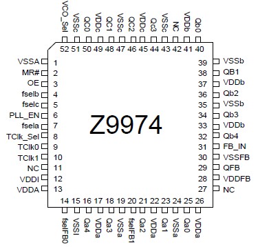
The Z9974 is a low cost 3.3V zero delay clock driver for high speed signal buffering and redistribution.
It provides the designer with the flexibility of selecting various Output/Input Frequency ratios selected by fsela, fselb, fselc, fselFB(0:1), and VCO_sel input settings.
The Z9974 integrates PLL technology for Zero delay propagation from Input to Output. The PLL feedback is externally available for propagation delay tuning and divide ratio alternatives as per table 1.
The Z9974 has three banks of outputs with independent divider stages. These dividers allow the banks to have different frequencies as per table 2.
TCLK0 and TCLK1 one are selectable input reference clocks and may be toggled dynamically during operation to provide modulation and phase shifting designs.
This device includes a Master Reset signal, which disables the outputs into Tristate (Hi-Z) mode, and reset all internal digital circuitry (excluding the PLL).
An Output Enable, OE, input pin is available for shutting Qa(0:4), Qb(0:4), and Qc(0:3) outputs in a low state. All outputs are held low with input clock turned off.
Input Voltage Relative to VSS: ........VSS-0.3V
Input Voltage Relative to VDD........ VDD+0.3V
Storage Temperature: .......-65°C to + 150°C
Operating Temperature:....... -40°C to +85°C
Maximum Power Supply:.............. 5.5V
This device contains circuitry to protect the inputs against damage due to high static voltages or electric field; however, precautions should be taken to avoid application of any voltage higher than the maximum rated voltages to this circuit. For proper operation, Vin and Vout should be constrained to the range: VSS<(Vin or Vout)<VDD
Unused inputs must always be tied to an appropriate logic voltage level (either VSS or VDD).
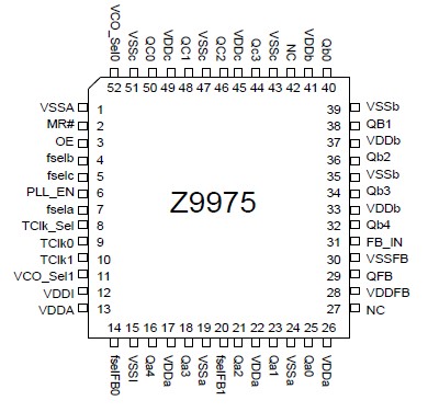
The Z9975 is a low cost 3.3V zero delay clock driver for high speed signal buffering and redistribution.
It provides the designer with the flexibility of selecting various Output/Input Frequency ratios selected by fsela, fselb, fselc, fselFB(0:1), and VCO_sel input settings.
The Z9975 integrates PLL technology for Zero delay propagation from Input to Output. The PLL feedback is externally available for propagation delay tuning and divide ratio alternatives as per table 1.
The Z9975 has three banks of outputs with independent divider stages. These dividers allow the banks to have different frequencies as per table 2.
TCLK0 and TCLK1 one are selectable input reference clocks and may be toggled dynamically during operation to provide modulation and phase shifting designs.
This device includes a Master Reset signal that disables the outputs into Tristate (Hi-Z) mode, and reset all internal digital circuitry (excluding the PLL).
An Output Enable, OE, input pin is available for shutting Qa(0:4), Qb(0:4), and Qc(0:3) outputs in a low state. All outputs are held low with input clock turned off.

Price: 4-6 USD
MT58L64L18CT-10 TQFP100

Price: 5-6.5 USD
DL-7140-211M laser tube

Price: 4-5 USD
74LVC74APG - IC FLIP FLOP D-Type POS-EDG DUAL 14TSSOP

Price: 6.5-8 USD
CYPRESS - Clock Synthesizer with Differential CPU Outputs

Price: 0.284-0.286 USD
PI5V330QEX Pericom Multiplexer Switch ICs

Price: 1-2 USD
IGBT power module, Single switch, 1200 V, Collector-emitter voltage, 430A

Price: 1-2 USD
a-Si TFT-LCD, NEC, 228.096Hmm, 560V

Price: 0.124-0.2 USD
PC354N1T - Mini-flat Package, AC Input Type Photocoupler - Sharp Electrionic Components

Price: 0.177-0.178 USD
RL1210JR51-XX-BL - Thick Film Chip Resistor Low Ohmic - TAITRON Components Incorporated

Price: 0.053-0.055 USD
STPS140A - POWER SCHOTTKY RECTIFIER - STMicroelectronics

Price: 1.45-1.5 USD
STA013 - MPEG 2.5 LAYER III AUDIO DECODER - STMicroelectronics

Price: 0.073-0.075 USD
SMBJ5347B - 5 Watt Surface Mount Silicon Zener Diodes - Micro Commercial Components

