Features: High-Integration Blocked Architecture
One 8 KB Boot Block w/Lock Out
Two 4 KB Parameter Blocks
One 112 KB Main Block
100,000 Erase/Program Cycles Per Block
Simplified Program and Erase
Automated Algorithms via On-Chip Write State Machine (WSM)
SRAM-Compatible Write Interface
Deep Power-Down Mode
0.05 mAICC Typical
0.8 mAIPP Typical
12.0V g5% VPP
High-Performance Read
70/75 ns, 90 ns, 120 ns, 150 ns Maximum Access Time
5.0V g10% VCC
Hardware Data Protection Feature
Erase/Write Lockout during PowerTransitions
Advanced Packaging, JEDEC Pinouts
32-Pin PDIP
32-Lead PLCC, TSOP
ETOXTM II Nonvolatile FlashTechnology
EPROM-Compatible Process Base
High-Volume Manufacturing Experience
Extended Temperature OptionsPinout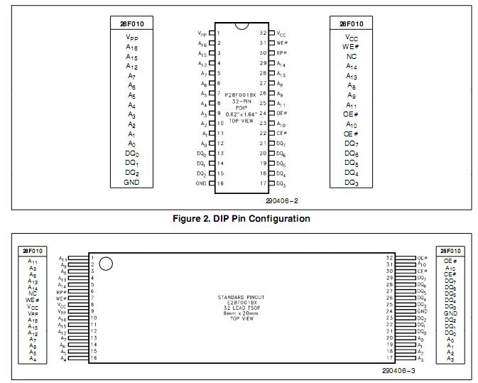 SpecificationsOperating Temperature
During Read ...............0to70(1)
During Erase/Program ..........0to70(1)
Operating Temperature
During Read ............-40to 85(2)
During Erase/Program .......-40to 85(2)
Temperature under Bias ........ -10to80(1)
Temperature under Bias ....... -20to 90(2)
Storage Temperature........... -65to125
Voltage on Any Pin
(except A9,RP,OE,VCC and VPP)
with Respect to GND ........ -2.0V to 7.0V(3)
Voltage on A9,RP, and OE
with Respect to GND .......-2.0V to 13.5V(3, 4)
VPP Program Voltage
with Respect to GND
During Erase/Program.......-2.0V to 14.0V(3, 4)
VCC Supply Voltage
with Respect to GND..........-2.0V to 7.0V(3)
Output Short Circuit Current...........100 mA(5)DescriptionIntel's 28F001BX-B and 28F001BX-T combine the cost-effectiveness of Intel standard flash memory with features that simplify write and allow block erase. These devices aid the system designer by combining the functions of several components into one, making boot block flash an innovative alternative to EPROM and EEPROM or battery-backed static RAM. Many new and existing designs can take advantage of the 28F001BX's integration of blocked architecture, automated electrical reprogramming, and standard processor interface.
The 28F001BX-B and 28F001BX-T are 1,048,576 bit nonvolatile memories organized as 131,072 bytes of 8 bits. They are offered in 32-pin plastic DIP, 32-lead PLCC and 32-lead TSOP packages. Pin assignment conform to JEDEC standards for byte-wide EPROMs. These devices use an integrated command port and state machine for simplified block erasure and byte reprogramming. The 28F001BX-T's block locations pro-vide compatibility with microprocessors and microcontrollers that boot from high memory, such as Intel's MCSÉ-186 family, 80286, i386TM, i486TM, i860TM and 80960CA. With exactly the same memory segmentation, the 28F001BX-B memory map is tailored for microprocessors and microcontrollers that boot from low memory,such as Intel's MCS-51, MCS-196, 80960KX and 80960SX families. All other features are identical, and unless otherwise noted, the term 28F001BX can refer to either device throughout the remainder of this document.
The boot block section includes a reprogramming write lock out feature to guarantee data integrity. 28F001BX-B is designed to contain secure code which will bring up the system minimally and download code to the other locations of the 28F001BX. Intel's 28F001BX employs advanced CMOS circuitry for systems requiring high-performance access speeds, low power consumption, and immunity to noise. Its access time provides no-WAIT-state performance for a wide range of microprocessors and microcontrollers. A deep-powerdown mode lowers power consumption to 0.25 mW typical through VCC, crucial in laptop computer, handheld instru-mentation and other low-power applications. The RPÝ power control input also provides absolute data protec- tion during system powerup or power loss.
Manufactured on Intel's ETOX process base, the 28F001BX-B builds on years of EPROM experience to yield the highest levels of quality, reliability, and cost-effectiveness.

 28F001BX-B Data Sheet


