DescriptionThe 2SC3241 is designed as NPN epitaxial planar type mitsubishi RF power transistor which is specifically designed for high power amplifiers in HF band.2SC3241 has five features. (1)High gain which would be larger than 12.3dB at f=30MHz, Vcc=12.5V and Pin=4W. (2)High ruggedness which me...
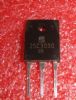
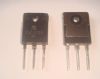
2SC3241: DescriptionThe 2SC3241 is designed as NPN epitaxial planar type mitsubishi RF power transistor which is specifically designed for high power amplifiers in HF band.2SC3241 has five features. (1)High ...
SeekIC Buyer Protection PLUS - newly updated for 2013!
268 Transactions
All payment methods are secure and covered by SeekIC Buyer Protection PLUS.
The 2SC3241 is designed as NPN epitaxial planar type mitsubishi RF power transistor which is specifically designed for high power amplifiers in HF band.
2SC3241 has five features. (1)High gain which would be larger than 12.3dB at f=30MHz, Vcc=12.5V and Pin=4W. (2)High ruggedness which means ability to withstand 20:1 load VSWR when operated at f=30MHz, Vcc=15.2V, Po=75W and Tc=25°C. (3)Emitter ballastend construction. (4)Low thermal resistance ceramic package with flange. (5)Input-output impedance Zin=0.5-j1.0(ohm), Zout=1.15-j1.4(ohm) at f=30MHz, Vcc=12.5V and Po=75W. Those are all the main features.
Some absolute maximum ratings of 2SC3241 have been concluded into several points as follow. (1)Its collector to base voltage would be 50V. (2)Its emitter to base voltage would be 5V. (3)Its collector to emitter voltage would be 20V. (4)Its collector current would be 18A. (5)Its collector dissipation would be 7.5W at Ta=25°C and would be 180W at Tc=25°C. (6)Its junction temperature would be 175°C. (7)Its storage temperature range would be from -55°C to 175°C. (8)Its thermal resistance would be 20°C/W for junction to ambient and would be 0.83°C/W for junction to case. It should be noted that stresses above those listed in absolute maximum ratings may cause permanent damage to device.
Also some electrical characteristics of 2SC3241 are concluded as follow. (1)Its emitter to base breakdown voltage would be min 5V. (2)Its collector to base breakdown voltage would be min 50V. (3)Its collector to emitter breakdown voltage would be min 20V. (4)Its collector cutoff current would be max 5mA. (5)Its emitter cutoff current would be max 4mA. (5)Its DC forward current gain would be min 10 and typ 50 and max 180. (6)Its output power would be min 75W and typ 85W. (7)Its collector efficiency would be min 55% and typ 65%. And so on. If you have any question or suggestion or want to know more information please contact us for details. Thank you!