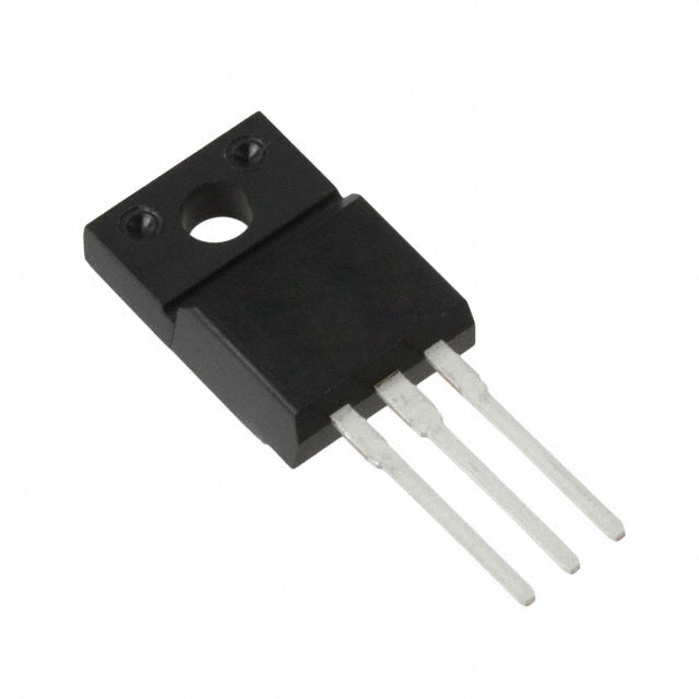
Features: SpecificationsDescription The 2SD2562 is a Silicon NPN Triple Diffused Planar Transistor(Complement to type 2SB1649) designed for Audio ,regulator and general purpose. The absolute maximun ratings of the 2SD2562 are at Ta=25°C, Collecto to Base Voltage VCBO is 150V;Collector to Emitter...
2SD2562: Features: SpecificationsDescription The 2SD2562 is a Silicon NPN Triple Diffused Planar Transistor(Complement to type 2SB1649) designed for Audio ,regulator and general purpose. The absolute maxim...
SeekIC Buyer Protection PLUS - newly updated for 2013!
268 Transactions
All payment methods are secure and covered by SeekIC Buyer Protection PLUS.
The 2SD2562 is a Silicon NPN Triple Diffused Planar Transistor(Complement to type 2SB1649) designed for Audio ,regulator and general purpose.
The absolute maximun ratings of the 2SD2562 are at Ta=25°C, Collecto to Base Voltage VCBO is 150V;Collector to Emitter Voltage VCEO is 150V;Emitter to Base Voltage VEBO is 5 V;Collector Current IC is 15A;collector power dissipation is 85W(Tc=25°C);Junction temperature 150°C maxnimum;Storage temperature is -55 to +150°C.
The outputs of the PWM are totem pole MOSFET gate drivers on the HDRIVE and LDRIVE pins. The outputs can sink approximately 1A and source 500mA. This characteristic optimizes the switching transi- tions by providing a controlled dV/dT at turn-on and a lower impedance at turn-off. These are complementary outputs with a typical deadtime of 200ns. Internal cir- cuitry prevents the possibility of simultaneous conduction of the output MOSFETs (shoot through). HDRIVE is the high side bootstrapped output. Its upper power supply rail is the BOOT pin which means that its output will fly ap- proximately 10V above VCC when the upper side of the totem pole output is conducting. The power supply rail for LDRIVE is CAP. As a result the Vgs of both gates are regulated to approximately 10V if VCC is >11V. A series resistor between these pins and the MOSFET gates of at least 10 ohms can be used to control ringing. Addition- ally, a low VF Schottky diode should be connected be- tween these pins and GND to prevent substrate conduction and possible erratic operation. Cathode-to-Anode Voltage Continuous Forward Current Continuous Forward Current Single Pulse Forward Current Maximum Single Pulse Avalanche Current ‚ Non-Repetitive Avalanche Energy ‚ Maximum Power Dissipation Maximum Power Dissipation Operating Junction and Storage Temperature Range Soldering Temperature, for 10 sec.
These devices are sensitive to electrostatic discharge; follow proper IC Handling Procedures. 1-888-INTERSIL or 321-724-7143 | Intersil (and design) is a registered trademark of Intersil Americas Inc. Copyright © Intersil Americas Inc. 2003. All Rights Reserved. All other trademarks mentioned are the property of their respective owners.These products are not designed for use in life support appliances, devices or systems where malfunction of these products can be reasonably expected to result in personal injury. Philips customers using or selling these products for use in such applications do so at their own risk and agree to fully indemnify Philips for any damages resulting from such improper use or sale.
At present there is not too much information about this model.If you are willing to find more about 2SD2562, please pay attention to our web! We will promptly update the relevant information.