Series: -
FET Type: MOSFET N-Channel, Metal Oxide
Transistor Type: -
Current - Collector (Ic) (Max): -
Voltage - Collector Emitter Breakdown (Max): -
Vce Saturation (Max) @ Ib, Ic: -
Current - Collector Cutoff (Max): -
DC Current Gain (hFE) (Min) @ Ic, Vce: -
Frequency - Transition: -
FET Feature: Standard
Current - Continuous Drain (Id) @ 25° C: 5A
Packaging: Tube
Mounting Type: Through Hole
Power - Max: 125W
Input Capacitance (Ciss) @ Vds: 700pF @ 25V
Gate Charge (Qg) @ Vgs: 60nC @ 10V
Drain to Source Voltage (Vdss): 1000V (1kV)
Vgs(th) (Max) @ Id: 3.5V @ 1mA
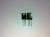
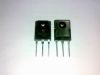
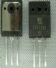
Package / Case: TO-3P-3, SC-65-3
Manufacturer: Toshiba
Supplier Device Package: TO-3P(N)
Rds On (Max) @ Id, Vgs: 3.8 Ohm @ 2A, 10V
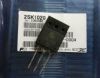
Features: SpecificationsDescription The 2SK1359 is designed as silicon N channel MOS type.Its typical application is DC−DC converter and motor drive applications.
2SK1359 has four features. The first one is about its low drain−source ON resistance which means RDS (ON) = 3.0 (typ.).The second one is about its high forward transfer admittance which means |Yfs| = 2.0 S (typ.).The third one is about its low leakage current which means IDSS = 300 A (max) (VDS = 800 V).The last one is about its enhancement mode which means Vth = 1.5~3.5 V (VDS = 10 V, ID = 1 mA).That are all the features.
Some absolute maximum ratings and electrical characteristics(Ta=25°C) of 2SK1359 have been concluded into several points as follow.The first one is about its drain−source voltage which would be 1000 V.The second one is about its drain−gate voltage (RGS = 20 k) which would be 1000 V.The third one is about its gate−source voltage which would be ±30 V.The fourth one is about its drain current which would be 5 A for DC and would be 15 A for pulse.The fifth one is about its drain power dissipation (Tc = 25°C) which would be 125 W.The sixth one is about its channel temperature which would be 150 °C.The seventh one is about its storage temperature range which would be from −55 to 150 °C.The eighth one is about its gate leakage current which would be ±50 nA(max) with text condition of Vgs = ±25 V, Vds = 0 V.The ninth one is about its drain cut−off current which would be 300 A(max) with test condition of Vds = 800 V, Vgs = 0 V.The last one is about its gate threshold voltage which would be with 1.5 to 3.5 V with test condition of Vds = 10 V, Id = 1 mA.For further information please contact us.
Also something should be noted that using continuously under heavy loads (e.g. the application of high temperature/current/voltage and the significant change in temperature, etc.) may cause this product to decrease in the reliability significantly even if the operating conditions (i.e.operating temperature/current/voltage, etc.) are within the absolute maximum ratings.
Parameters: | Technical/Catalog Information | 2SK1359 |
| Vendor | Toshiba |
| Category | Discrete Semiconductor Products |
| Mounting Type | Through Hole |
| FET Polarity | N-Channel |
| Drain to Source Voltage (Vdss) | 1000V (1kV) |
| Current - Continuous Drain (Id) @ 25° C | 5A |
| Rds On (Max) @ Id, Vgs | 3.8 Ohm @ 2A, 10V |
| Input Capacitance (Ciss) @ Vds | 700pF @ 25V |
| Power - Max | 125W |
| Packaging | Tube |
| Gate Charge (Qg) @ Vgs | 60nC @ 10V |
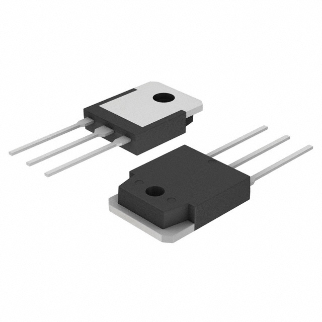
| Package / Case | 2-16C1B (TO-247 N) |
| FET Feature | Standard |
| Lead Free Status | Contains Lead |
| RoHS Status | RoHS Non-Compliant |
| Other Names | 2SK1359
2SK1359
|
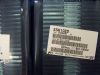
 2SK1359 Data Sheet