Series: -
FET Type: MOSFET N-Channel, Metal Oxide
Transistor Type: -
Current - Collector (Ic) (Max): -
FET Feature: Logic Level Gate
Voltage - Collector Emitter Breakdown (Max): -
Vce Saturation (Max) @ Ib, Ic: -
Current - Collector Cutoff (Max): -
DC Current Gain (hFE) (Min) @ Ic, Vce: -
Frequency - Transition: -
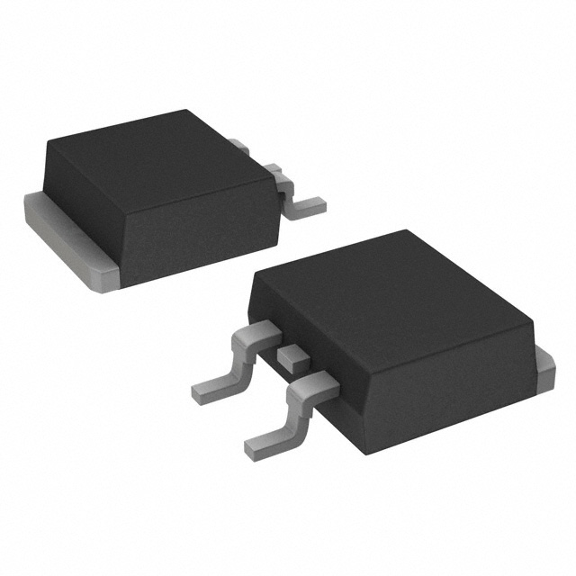
Mounting Type: Surface Mount
Drain to Source Voltage (Vdss): 60V
Gate Charge (Qg) @ Vgs: 12nC @ 10V
Current - Continuous Drain (Id) @ 25° C: 5A
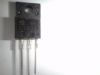
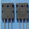
Package / Case: TO-252-3, DPak (2 Leads + Tab), SC-63
Power - Max: 20W
Packaging: Bulk
Vgs(th) (Max) @ Id: 2V @ 1mA
Input Capacitance (Ciss) @ Vds: 370pF @ 10V
Manufacturer: Toshiba
Rds On (Max) @ Id, Vgs: 160 mOhm @ 2.5A, 10V
Supplier Device Package: PW-MOLD
Application4 V gate drive
Low drain−source ON-resistance : RDS (ON) = 0.12 (typ.)
High forward transfer admittance : |Yfs| = 5.0 S (typ.)
Low leakage current : IDSS = 100 A (max) (VDS = 60 V)
Enhancement mode : Vth = 0.8~2.0 V (VDS = 10 V, ID = 1 mA)Specifications
| Characteristics |
Symbol |
Rating |
Unit |
| Drain-source voltage |
VDSS |
60 |
V |
| Drain?gate voltage (RGS = 20 k) |
VDGR |
60 |
V |
| Gate?source voltage |
VGSS |
±20 |
V |
| Drain current |
DC (Note 1) |
ID |
5 |
A
|
| Pulse (Note 1) |
IDP |
20 |
| Drain power dissipation (Tc = 25) |
PD |
20 |
W |
Single pulse avalanche energy
(Note 2) |
EAS |
129 |
mJ |
| Avalanche current |
IAR |
5 |
A |
| Repetitive avalanche energy (Note 3) |
EAR |
2 |
mJ |
| Channel temperature |
Tch |
150 |
|
| Storage temperature range |
TSTG |
-55 ~ 150 |
|
Note: Using continuously under heavy loads (e.g. the application of high temperature/current/voltage and the significant change in temperature, etc.) may cause this product to decrease in the reliability significantly even if the operating conditions (i.e. operating temperature/current/voltage, etc.) are within the absolute maximum ratings. Please design the appropriate reliability upon reviewing the Toshiba Semiconductor Reliability Handbook ("Handling Precautions"/Derating Concept and Methods) and individual reliability data (i.e. reliability test report and estimated failure rate, etc).
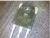
Parameters: | Technical/Catalog Information | 2SK2231 |
| Vendor | Toshiba |
| Category | Discrete Semiconductor Products |
| Mounting Type | Through Hole |
| FET Polarity | N-Channel |
| Drain to Source Voltage (Vdss) | 60V |
| Current - Continuous Drain (Id) @ 25° C | 5A |
| Rds On (Max) @ Id, Vgs | 160 mOhm @ 2.5A, 10V |
| Input Capacitance (Ciss) @ Vds | 370pF @ 10V |
| Power - Max | 20W |
| Packaging | Bulk |
| Gate Charge (Qg) @ Vgs | 12nC @ 10V |
| Package / Case | 2-7B1B |
| FET Feature | Logic Level Gate |
| Lead Free Status | Contains Lead |
| RoHS Status | RoHS Non-Compliant |
| Other Names | 2SK2231
2SK2231
|
 2SK2231 Data Sheet