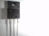
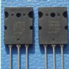
Features: SpecificationsDescription The 2SK2363/2SK2364 is N-Channel MOS Field Effect Transistor designed for high voltage switching applications.The 2SK2363/2SK2364 has 3 features including Low on-resistance,2SK2363: RDS (on) = 0.5 (VGS = 10 V, ID = 4.0 A),2SK2364: RDS (on) = 0.6 (VGS = 10 V, ID = 4.0 A);Low Ciss Ciss = 1600 pF TYP;High Avalanche Capability Ratings;Isolate TO-220 Package.
The absolute maximun ratings of the 2SK2363/2SK2364 are at Ta=25°C, Drain to source voltage(2SK2363/2SK2364 ) VDSS is 450/500V;Gate to source voltage VGSS is ±30V;drain Current ID(DC) is ±8.0A;total power dissipation is 35W;channel temperature is 150°C maxnimum;Storage temperature is -55 to +150°C.
When accessing the 2SK2364, the user addresses 512 locations each with 8 data bits. These data bits are shifted serially. The addresses are accessed using the SPI protocol, which includes a chip select (to permit multiple devices on the bus), an op-code including the upper address bit, and a word address. The word address consists of the lower 8-addres bits. The complete address of 9-bits specifies each byte address uniquely. The preamplifier output then feeds the mixer stage where the required channel is image reject downconverted to the IF frequency. The local oscillator frequency for the downconversion is obtained from the on board local oscillator, which uses an external varactor tuned tank. Typical VCO applications are contained in Figures 8, 9 and 10. Normally the signal source for the LM1881 is assumed to be clean and relatively noise-free, but some sources may have excessive video peaking, causing high frequency video and chroma components to extend below the black level refer- ence. Some video discs keep the chroma burst pulse present throughout the vertical blanking period so that the burst actually appears on the sync tips for three line periods instead of at black level. A clean composite sync signal can be generated from these sources by filtering the input signal. When the source impedance is low, typically 75, a 620 resistor in series with the source and a 510 pF capacitor to ground will form a low pass filter with a corner frequency of 500 kHz. This bandwidth is more than sufficient to pass the sync pulse portion of the waveform; however, any subcarrier content in the signal will be attenuated by almost 18 dB, effectively taking it below the comparator threshold. Filtering will also help if the source is contaminated with thermal noise. The output waveforms will become delayed from be- tween 40 ns to as much as 200 ns due to this filter. This much delay will not usually be significant but it does contrib- ute to the sync delay produced by any additional signal processing. Since the original video may also undergo pro- cessing, the need for time delay correction will depend on the total system, not just the sync stripper.
The diode connected between the gate and source of the transistor serves as a protector against ESD. When this device is actually used, an additional protection circuit is externally required if a voltage exceeding the rated voltage may be applied to this device.
At present there is not too much information about this model.If you are willing to find more about 2SK2363/2SK2364 , please pay attention to our web! We will promptly update the relevant information.

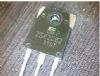
 2SK2363/2SK2364 Data Sheet