33702

Features: • Operating Voltage: 2.8 V to 6.0 V• High-Accuracy Output Voltages• Fast Transient Response• Switcher Output Current Up to 3.0 A• Undervoltage Lockout• Power Sequencing• Programmable Watchdog Timer• Voltage Margining via I2C™ Bus̶...

product image

33702 Picture
SeekIC No. : 004228517 Detail

33702: Features: • Operating Voltage: 2.8 V to 6.0 V• High-Accuracy Output Voltages• Fast Transient Response• Switcher Output Current Up to 3.0 A• Undervoltage Lockout• ...

floor Price/Ceiling Price

Part Number:
33702
Supply Ability:
5000

Price Break

  • Qty
  • 1~5000
  • Unit Price
  • Negotiable
  • Processing time
  • 15 Days
Total Cost: $ 0.00

SeekIC Buyer Protection PLUS - newly updated for 2013!

  • Escrow Protection.
  • Guaranteed refunds.
  • Secure payments.
  • Learn more >>

Month Sales

268 Transactions

Rating

evaluate  (4.8 stars)

Upload time: 2024/4/26

Payment Methods

All payment methods are secure and covered by SeekIC Buyer Protection PLUS.

Notice: When you place an order, your payment is made to SeekIC and not to your seller. SeekIC only pays the seller after confirming you have received your order. We will also never share your payment details with your seller.
Product Details

Description


Features:

• Operating Voltage: 2.8 V to 6.0 V
• High-Accuracy Output Voltages
• Fast Transient Response
• Switcher Output Current Up to 3.0 A
• Undervoltage Lockout
• Power Sequencing
• Programmable Watchdog Timer
• Voltage Margining via I2C™ Bus
• Overcurrent Protection
• Reset with Programmable Power-ON Delay
• Enable Inputs


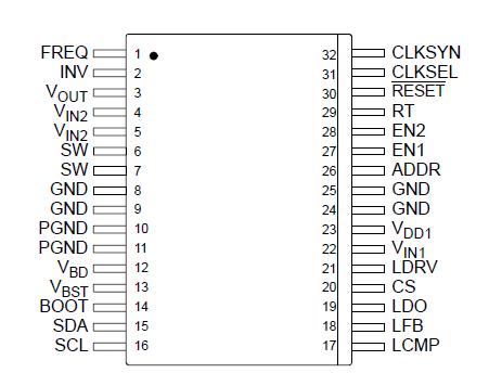
Pinout

  Connection Diagram


Specifications

Rating Symbol Value Unit
Supply Voltage VIN1, VIN2 -0.3 to 7.0 V
Switching Node SW -1.0 to 7.0 V
Buck Regulator Bootstrap Input (BOOT - SW) BOOT -0.3 to 8.5 V
Boost Regulator Output VBST -0.3 to 8.5 V
Boost Regulator Drain VBD -0.3 to 9.5 V
RESET Drain Voltage RESET -0.3 to 7.0 V
Enable Pins (EN1, EN2) -0.3 to 7.0 V
Logic Pins (SDA, SCL, CLKSYN) -0.3 to 7.0 V
Analog Pins (INV, VOUT, RESET) -0.3 to 7.0 V
Analog Pins (LDRV, LFB, LDO, LCMP, CS) -0.3 to 8.5 V
Analog Pins (CLKSEL, ADDR, RT, FREQ, VDDI) -0.3 to 3.6 V
ESD Voltage
Human Body Model (Note 1)
Machine Model (Note 2)
VESD1
VESD2
±2000
±200
V
Storage Temperature TSTG -65 to 150 °C
Power Dissipation (TA = 85°C) (Note 3) PD TBD W
Lead Soldering Temperature (Note 4) TSOLDER 260 °C
Maximum Junction Temperature TJMAX 125 °C
Thermal Resistance, Junction to Ambient (Note 5) RJA 68 °C/W
Thermal Resistance, Junction to Base (Note 6) RJB 18 °C/W


Customers Who Bought This Item Also Bought

Margin,quality,low-cost products with low minimum orders. Secure your online payments with SeekIC Buyer Protection.
Crystals and Oscillators
Connectors, Interconnects
Optical Inspection Equipment
Isolators
LED Products
View more