Features: Data input, address, byte enable and control registers
Self-timed write allows fast cycle time
Separate byte controls for multiplexed bus and bus matching compatibility
Dual Cycle Deselect (DCD) for Pipelined Output Mode
2.5V (±100mV) power supply for core
LVTTL compatible, selectable 3.3V (±150mV) or 2.5V (±100mV) power supply for I/Os and control signals on each port
Industrial temperature range (-40°C to +85°C) is available at 166MHz and 133MHz
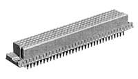
Available in a 256-pin Ball Grid Array (BGA), a 208-pin
Plastic Quad Flatpack (PQFP) and 208-pin fine pitch Ball
Grid Array (fpBGA)
Supports JTAG features compliant with IEEE 1149.1
Due to limited pin count JTAG is not supported on the 208- pin PQFP package
Features:
True Dual-Port memory cells which allow simultaneous access of the same memory location
High-speed data access
Commercial: 3.4 (200MHz)/3.6ns (166MHz)/
4.2ns (133MHz)(max.)
Industrial: 3.6ns (166MHz)/4.2ns (133MHz) (max.)
Selectable Pipelined or Flow-Through output mode
Counter enable and repeat features
Dual chip enables allow for depth expansion without additional logic
Interrupt and Collision Detection Flags
Full synchronous operation on both ports
5ns cycle time, 200MHz operation (14Gbps bandwidth)
Fast 3.4ns clock to data out
1.5ns setup to clock and 0.5ns hold on all control, data, and address inputs @ 200MHz
Pinout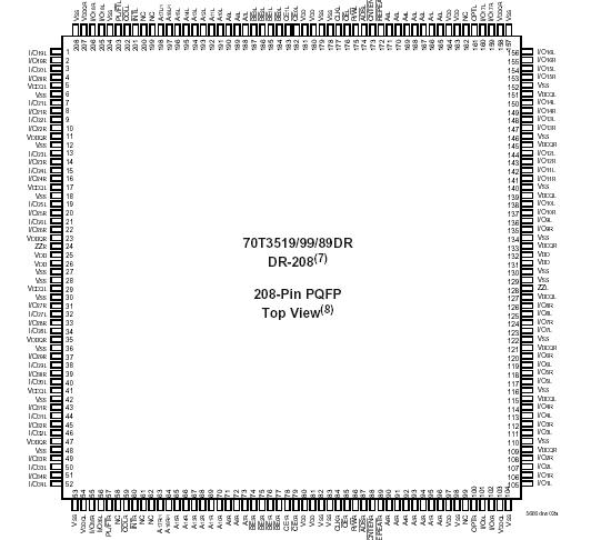 NOTES:
1. Pin is a NC for IDT70T3599 and IDT70T3589.
2. Pin is a NC for IDT70T3589.
3. All VDD pins must be connected to 2.5V power supply.
4. All VDDQ pins must be connected to appropriate power supply: 3.3V if OPT pin for that port is set to VDD (2.5V), and 2.5V if OPT pin for that port is set to Vss (0V).
5. All VSS pins must be connected to ground supply.
6. Package body is approximately 28mm x 28mm x 3.5mm.
7. This package code is used to reference the package diagram.
8. This text does not indicate orientation of the actual part-marking.
9. Due to limited pin count, JTAG is not supported in the DR-208 package.
10. Pins 162 and 99 will be VREFL and VREFR respectively for future HSTL device.
Specifications
|
Symbol |
Rating |
Commercial
& Industrial
|
Unit |
|
VTERM
(VDD) |
VDD Terminal Voltage
with Respect to GND |
-0.5 to 3.5 |
V |
|
VTERM(2)
(VDDQ) |
VDDQ Terminal Voltage
with Respect to GND |
-0.3 to VDDQ + 0.3 |
V |
|
VTERM(2)
(INPUTS and I/O's) |
Input and I/O Terminal
Voltage with Respect to GND |
-0.3 to VDDQ + 0.3
|
V |
|
TBIAS(3) |
Temperature Under Bias |
-55 to +125
|
°C |
|
TSTG |
Storage Temperature |
-65 to +150
|
°C |
|
TJN |
Junction Temperature |
+ 150
|
°C |
|
IOUT(For VDDQ = 3.3V) |
DC Output Current |
50
|
mA |
|
IOUT(For VDDQ = 2.5V) |
DC Output Current |
40
|
mA |
NOTES:
1. Stresses greater than those listed under ABSOLUTE MAXIMUM RATINGS may cause permanent damage to the device. This is a stress rating only and functional operation of the device at these or any other conditions above those indicated in the operational sections of this specification is not implied. Exposure to absolute maximum rating conditions for extended periods may affect reliability.
2. This is a steady-state DC parameter that applies after the power supply has reached its nominal operating value. Power sequencing is not necessary; however, the voltage on any Input or I/O pin cannot exceed VDDQ during power supply ramp up.
3. Ambient Temperature under DC Bias. No AC Conditions. Chip Deselected.
DescriptionThe IDT70T3519/99/89 is a high-speed 256/128/64K x 36 bit synchronous Dual-Port RAM. The memory array utilizes Dual-Port memory cells to allow simultaneous access of any address from both ports. Registers on control, data, and address inputs provide minimal setup and hold times.
The timing latitude provided by this approach allows systems to be designed with very short cycle times. With an input data register, the IDT70T3519/99/89 has been optimized for applications having unidirectional or bidirectional data flow in bursts. An automatic power down feature, controlled by CE0 and CE1, permits the on-chip circuitry of each port to enter a very low standby power mode. The IDT70T3519/99/89can support an operating voltage of either 3.3V or 2.5V on one or both ports, controllable by the OPT pins. The power supply for the core of the device (VDD) is at 2.5V.

 40865 Data Sheet