Features: • 0.5 MICRON CMOS Technology
• Guaranteed low skew < 500ps (max.)
• Very low duty cycle distortion < 1.0ns (max.)
• Very low CMOS power levels
• TTL compatible inputs and outputs
• Inputs can be driven from 3.3V or 5V components
• Two independent output banks with 3-state control
• 1:5 fanout per bank
• "Heartbeat" monitor output
• VCC = 3.3V ± 0.3V
• Available in SSOP, SOIC, and QSOP packagesPinout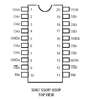 Specifications
|
Symbol |
Rating |
Commercial
& Industrial
|
Unit |
|
VTERM |
Terminal Voltage with respect to GND |
-0.5 to +4.6 |
V |
|
VTERM |
Terminal Voltage with Respect to GND |
0.5 to +7 |
V |
|
VTER(2) |
Terminal Voltage with Respect to GND |
0.5 to VCC+0.5 |
°C |
|
TSTG |
Storage
Temperature |
65 to +150
|
°C |
|
IOUT |
DC Output Current |
60 to +60
|
mA |
NOTES:
1. Stresses greater than those listed under ABSOLUTE MAXIMUM RATINGS may cause
permanent damage to the device. This is a stress rating only and functional operation
of the device at these or any other conditions above those indicated in the operational
sections of this specification is not implied. Exposure to absolute maximum rating
conditions for extended periods may affect reliability.
2. VCC terminals.
3. Input terminals.
4. Outputs and I/O terminals
DescriptionThe FCT3805 is a 3.3 volt, non-inverting clock driver built using advanced dual metal CMOS technology. The device consists of two banks of drivers, each with a 1:5 fanout and its own output enable control. The FCT3805 has a "heartbeat" monitor for diagnostics and PLL driving. The MON output is identical to all other outputs and complies with the output specifications in this document.
The FCT3805 offers low capacitance inputs with hysteresis. The FCT3805 is designed for high speed clock distribution where signal quality and skew are critical. The FCT3805 also allows single point-topoint transmission line driving in applications such as address distribution, where one signal must be distributed to multiple recievers with low skew and high signal quality.

 40917 Data Sheet