Shape: Rectangular
Length: 4' (1.22m)
Material: Rubber
Manufacturer: Desco
Mat Type: Floor
Color: Black
Width: 3' (0.91m)
Thickness: 0.50" (12.70mm)
Features: Anti Fatigue, Conductive
Series: Statfree i™
Features: • Operates at 3.3V VDD/AVDD and 2.5V/3.3V VDDQ
• 1:10 fanout
• 3-level inputs for output control
• External feedback (FBIN) pin is used to synchronize the
outputs to the clock input signal
• No external RC network required for PLL loop stability
• Configurable 2.5V or 3.3V LVTTL outputs
• tPD Phase Error at 100MHz to 166MHz: ±150ps
• Jitter (peak-to-peak) at 133MHz and 166MHz: ±75ps
• Spread spectrum compatible
• Operating Frequency:
− Std: 25MHz to 140MHz
− A: 25MHz to 167MHz
• Available in TSSOP packagePinout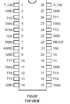 Specifications
|
Rating |
Symbol |
Value |
unit |
|
Supply Voltage Range |
V CC1, VCC2 |
0.5 to +4.6
|
V |
|
Input Voltage Range |
VI (2)
|
0.5 to +5.5 |
V |
|
Collector Current (Pin 10) |
VO(2) |
0.5 to
VDD+0.5
|
V |
|
Voltage Range applied to any
output in the HIGH or LOW state
|
IIK (VI < 0)
|
50 |
mA |
|
Input Clamp Current |
IOK
(VO < 0 or VO > VDD) |
±50
|
mA |
|
Output Clamp Current |
IO
(VO = 0 to VDD)
|
±50 |
mA |
|
Continuous Output Current |
IRES |
±200 |
mA |
|
Continuous Current |
VDD or GND |
65 to +150 |
mA |
|
Storage Temperature Range |
TSTG |
5.0 |
°C |
|
Junction Temperature |
TJ |
+150 |
°C |
NOTES:
1. Stresses greater than those listed under ABSOLUTE MAXIMUM RATINGS may cause
permanent damage to the device. This is a stress rating only and functional operation
of the device at these or any other conditions above those indicated in the operational
sections of this specification is not implied. Exposure to absolute maximum rating
conditions for extended periods may affect reliability.
2. The input and output negative-voltage ratings may be exceeded if the input and output
clamp-current ratings are observed.
3. The maximum package power dissipation is calculated using a junction temperature
of 150°C and a board trace length of 750 mils.DescriptionThe IDT5V2528 inputs, PLL core, Y0, Y1, and FBOUT buffers operate from the 3.3V VDD and AVDD power supply pins. One bank of ten outputs provide low-skew, low-jitter copies of CLK. Of the ten outputs, up to seven may be configured for 2.5V or 3.3V LVTTL outputs. The number of 2.5V outputs is controlled by 3-level input signals G_Ctrl and T_Ctrl, and by connecting the appropriate VDDQ pins to 2.5V or 3.3V. The 3-level input signals of IDT5V2528 may be hard-wired to high-mid-low levels. Output signal duty cycles are adjusted to 50 percent, independent of the duty cycle at CLK. The outputs can be enabled or disabled via the G_Ctrl input. When the G_Ctrl input is mid or high, the outputs switch in phase and frequency with CLK; when the G_Ctrl is low, all outputs (except FBOUT) are disabled to the logic-low state.
Unlike many products containing PLLs, the IDT5V2528 does not require external RC networks. The loop filter for the PLL is included on-chip, minimizing component count, board space, and cost. Because it is based on PLL circuitry, the IDT5V2528 requires a stabilization time to achieve phase lock of the feedback signal to the reference signal. This stabilization time is required, following power up and application of a fixed-frequency, fixed-phase signal at CLK, as well as following any changes to the PLL reference or feedback signals.
The IDT5V2528 PLL can be bypassed for test purposes by strapping AVDD to ground.
 40931 Data Sheet