SeekIC No. : 004233392
Detail
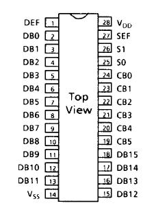
54HSCT630: Features: *Radiation Hard: Dose Rate Upset Exceeding 3x10¹⁰ Rad(Si)/sec Total Dose for Functionality Upto 1x10⁶ Rad(Si)*High SEU Immunity, Latch Up Free*CMOS-SOS Technology*All Inputs and Outputs Fu...
 54HSCT630 Data Sheet
floor Price/Ceiling Price
- Part Number:
- 54HSCT630
- Supply Ability:
- 5000
Price Break
- Qty
- 1~5000
- Unit Price
- Negotiable
- Processing time
- 15 Days
SeekIC Buyer Protection PLUS - newly updated for 2013!
- Escrow Protection.
- Guaranteed refunds.
- Secure payments.
- Learn more >>
Month Sales
268 Transactions
Payment Methods
All payment methods are secure and covered by SeekIC Buyer Protection PLUS.
Notice: When you place an order, your payment is made to SeekIC and not to your seller. SeekIC only pays the seller after confirming you have received your order. We will also never share your payment details with your seller.