5815

Features: *To 4.4 MHz Date-lnput Rate* High-Voltage Source Outputs* CMOS, NMOS, TTL Compatible Inputs* Low-Power CMOS Latches* Internal Pull-Down Resistors* Wide Supply-Voltage RangePinoutSpecificationsOutput Voltage, VOUT . . . . . . . . . . . . . . 60 VLogic Supply Voltage Range, VDD . . . . . ....

product image

5815 Picture
SeekIC No. : 004233972 Detail

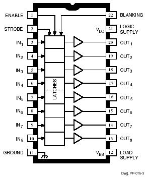
5815: Features: *To 4.4 MHz Date-lnput Rate* High-Voltage Source Outputs* CMOS, NMOS, TTL Compatible Inputs* Low-Power CMOS Latches* Internal Pull-Down Resistors* Wide Supply-Voltage RangePinoutSpecificat...

floor Price/Ceiling Price

Part Number:
5815
Supply Ability:
5000

Price Break

  • Qty
  • 1~5000
  • Unit Price
  • Negotiable
  • Processing time
  • 15 Days
Total Cost: $ 0.00

SeekIC Buyer Protection PLUS - newly updated for 2013!

  • Escrow Protection.
  • Guaranteed refunds.
  • Secure payments.
  • Learn more >>

Month Sales

268 Transactions

Rating

evaluate  (4.8 stars)

Upload time: 2024/4/28

Payment Methods

All payment methods are secure and covered by SeekIC Buyer Protection PLUS.

Notice: When you place an order, your payment is made to SeekIC and not to your seller. SeekIC only pays the seller after confirming you have received your order. We will also never share your payment details with your seller.
Product Details

Description


Features:

* To 4.4 MHz Date-lnput Rate
* High-Voltage Source Outputs
* CMOS, NMOS, TTL Compatible Inputs
* Low-Power CMOS Latches
* Internal Pull-Down Resistors
* Wide Supply-Voltage Range


Pinout

  Connection Diagram


Specifications

Output Voltage, VOUT . . . . . . . . . . . . . . 60 V
Logic Supply Voltage Range,
   VDD . . . . . . . . . . . . . .... . . . . 4.5 V to 15 V
Load Supply Voltage Range,
   VBB . . . . . . . . . . . . . . .... . . . 5.0 V to 60 V
Input Voltage Range,
   VIN . . . . . . . . ...... . . -0.3 V to VDD + 0.3 V
Continuous Output Current,
   IOUT . . . . . . . . . ... . . . . . . . . . . . . -40 mA
Package Power Dissipation, PD
   (UCN5815A) . . . . . .... . ... . . . . . . . 2.5 W*
   (UCN5815EP) . . . . . . ...... . . . . . . 2.27 W*
Operating Temperature Range,
   TA . . . . . . . . . . . . ...... . . . . -20 to +85
Storage Temperature Range,
   TS . . . . . . . . . . . . ...... . . . -55 to +150


Description

Designed primarily for use with high-voltage vacuum-fluorescent displays, the UCN5815A and UCN5815EP BiMOS II integrated circuits consist of eight npn Darlington source drivers with output pulldown resistors, a CMOS latch for each driver, and common STROBE, BLANKING, and ENABLE functions.

BiMOS II devices UCN5815A and UCN5815EP  have considerably better data-input rates than the original BiMOS circuits. With a 5 V logic supply, they will operate to at least 4.4 MHz. With a 12 V supply, significantly higher speeds are obtained. The CMOS inputs of UCN5815A and UCN5815EP cause minimum loading and are compatible with standard CMOS and NMOS logic commonly found in microprocessor designs. TTL circuits may require the use of appropriate pull-up resistors.

The bipolar outputs of UCN5815A and UCN5815EP  may be used as segment, dot (matrix), bar, or digit drivers in vacuum-fluorescent displays. All eight outputs can be activated simultaneously at ambient temperatures in excess of 75°C. To simplify printed wiring board layout, output connections of UCN5815A and UCN5815EP  are opposite the inputs. A minimum component display subsystem, requiring few or no discrete components, can be assembled using the UCN5815A/EP with the UCN5810AF/EPF/LWF, UCN5812AF/EPF, or UCN5818AF/EPF serial-to-parallel latched drivers.

Suffix 'A' devices are furnished in a standard 22-pin plastic DIP; suffix 'EP' indicates a 28-lead PLCC.


Customers Who Bought This Item Also Bought

Margin,quality,low-cost products with low minimum orders. Secure your online payments with SeekIC Buyer Protection.
Isolators
Audio Products
LED Products
Potentiometers, Variable Resistors
View more