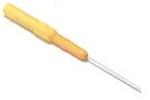
Tip Style
: Spear
Equipment Type
: Back Probe Pins
Features: - Output voltage adjustable from 5V to 20V
- Dropout voltage typically 0.5V @ Io = 1A
- Output current in excess of 1A
- Trimmed reference voltage
- Reverse battery protection
- Internal short circuit current limit
- Mirror image insertion protection
- TTL, CMOS compatible ON/OFF switch
- CONTROLLING DOCUMENT
LM2941J/883 5962-9166701QEA
LM2941K/883 5962-9166701QXA
LM2941WG/883 5962-9166701QYA SpecificationsInput Voltage (Survival Voltage < 100mS)
60V
Internal Power Dissipation
(Note 2, 3)
Internally Limited
Maximum Junction Temperature
150 C
Storage Temperature Range
-65 C < TA < +150 C
Lead Temperature
(Soldering, 10 seconds) 300 C
Thermal Resistance
ThetaJA
T03 Pkg (Still Air) 40 C/W
T03 Pkg (500LF/Min Air Flow) TBD
CERDIP (Still Air) 73 C/W
CERDIP (500LF/Min Air Flow) 37 C/W
CERAMIC SOIC (Still Air) 122 C/W
CERAMIC SOIC (500LF/Min Air Flow) 77 C/W
ThetaJC
(Note 3)
T03 Pkg 5 C/W
CERDIP (Note 3 applicable to this Pkg only) 3 C/W
CERAMIC SOIC 5 C/W
Package Weight
(Typcial)
T03 TBD
CERDIP 1970mg
CERAMIC SOIC 360mg
ESD Susceptibility
(Note 4)
500V
Note 1: Absolute Maximum Ratings indicate limits beyond which damage to the device may occur.Operating Ratings indicate conditions for which the device is functional, but do not guarantee specific performance limits. For guaranteed specifications and test conditions, see the Electrical Characteristics. The guaranteed specifications apply only for the test conditions listed. Some performance characteristics may degrade when the device is not operated under the listed test conditions.
Note 2: The maximum power dissipation must be derated at elevated temperatures and is dictated by Tjmax (maximum junction temperature), ThetaJA (package junction to ambient thermal resistance), and TA (ambient temperature). The maximum allowable power dissipation at any temperature is Pdmax = (Tjmax - TA)/ThetaJA or the number given in the Absolute Maximum Ratings, whichever is lower.
Note 3: The package material for these devices allows much improved heat transfer over our standard ceramic packages. In order to take full advantage of this improved heat transfer, heat sinking must be provided between the package base (directly beneath the die), and either metal traces on, or thermal vias through, the printed circuit board. Without this additional heat sinking, device power dissipation must be calculated using junction-to-ambient, rather than junction-to-case, thermal resistance. It must not be assumed that the device leads will provide substantial heat transfer out of the package, since the thermal resistance of the leadframe material is very poor, relative to the material of the package base. The stated junction-to-case thermal resistance is for the package material only, and does not account for the additional thermal resistance between the package base and the printed circuit board. The user must determine the value of the additional thermal resistance and must combine this with the stated value for the package, to calculate the total allowed power dissipation for the device.
Note 4: Human body model, 100pF discharged through 1.5K Ohms.
DescriptionThe 6411 positive voltage regulator features the ability to source 1A of output current with a typical dropout voltage of 0.5V and a maximum of 1V over the entire temperature range. Furthermore, a quiescent current reduction circuit has been included which reduces the ground pin current when the differential between the input voltage and the output oltage exceeds approximately 3V. The quiescent current with 1A of output current and an input-output differential of 5V is therefore only 30mA. Higher quiescent currents only exist when the regulator is in the dropout mode (Vin - Vout < 3V).
Designed also for vehicular applications, the 6411 and all regulated circuitry are protected from reverse battery installations or two-battery jumps. During line transients,such as load dump when the input voltage can momentarily exceed the specified maximum operating voltage, the 6411 will automatically shut down to protect both the internal circuits and the load. Familiar regulator features such as short circuit and thermal overload protection are also provided.
Parameters: | Technical/Catalog Information | 6411 |
| Vendor | Crydom |
| Category | Relays, I/O Modules |
| Mounting Type | Through Hole |
| Mounting Type | Socket |
| Type | AC Output Module |
| Output Type | 12 ~ 140VAC |
| Circuit | SPST-NC |
| Switch Function | On-Off |
| Contact Rating @ Voltage | 3.5A @ 140VAC |
| Control Voltage | 5.000 VDC [Typ] |
| Termination Style | PC Pin |
| Termination Style | Socketable |
| Control Range | 3.500 VDC [Min] |
| Control Range | 6.000 VDC [Max] |
| Output Voltage | 12.000 VAC [Min] |
| Output Voltage | 140.000 VAC [Max] |
| Operating Temperature | -40 °C [Min] |
| Operating Temperature | 80 °C [Max] |
| Input Current | 0.100 mA [Max] |
| Output Current | 0.02 A [Min] |
| Output Current | 3.50 A [Max] |
| Height | 31.700 mm [Typ] |
| Length | 43.100 mm [Typ] |
| Width | 15.200 mm [Typ] |
| Lead Free Status | Lead Free |
| RoHS Status | RoHS Compliant |
| Other Names | 6411
6411
CC1241 ND
CC1241ND
CC1241
|
 6411 Data Sheet