703025A

Features: •Number of instructions: 74•Minimum instruction execution time: 30 ns (@ 33 MHz operation)•General-purpose registers: 32 bits ´ 32 registers•Instruction set optimized for control applications•On-chip memory ROM: 256 KB (PD703025A) 128 KB (PD703003A) 96...

product image

703025A Picture
SeekIC No. : 004239818 Detail

703025A: Features: •Number of instructions: 74•Minimum instruction execution time: 30 ns (@ 33 MHz operation)•General-purpose registers: 32 bits ´ 32 registers•Instruction set o...

floor Price/Ceiling Price

Part Number:
703025A
Supply Ability:
5000

Price Break

  • Qty
  • 1~5000
  • Unit Price
  • Negotiable
  • Processing time
  • 15 Days
Total Cost: $ 0.00

SeekIC Buyer Protection PLUS - newly updated for 2013!

  • Escrow Protection.
  • Guaranteed refunds.
  • Secure payments.
  • Learn more >>

Month Sales

268 Transactions

Rating

evaluate  (4.8 stars)

Upload time: 2024/4/27

Payment Methods

All payment methods are secure and covered by SeekIC Buyer Protection PLUS.

Notice: When you place an order, your payment is made to SeekIC and not to your seller. SeekIC only pays the seller after confirming you have received your order. We will also never share your payment details with your seller.
Product Details

Description


Features:

•Number of instructions: 74
•Minimum instruction execution time: 30 ns (@ 33 MHz operation)
•General-purpose registers: 32 bits ´ 32 registers
•Instruction set optimized for control applications
•On-chip memory ROM: 256 KB (PD703025A) 128 KB (PD703003A) 96 KB (PD703004A) RAM: 8 KB (PD703025A) 4 KB (PD703003A, 703004A)
•Advanced on-chip interrupt controller
•Real-time pulse unit suitable for control operations
•Powerful serial interface (on-chip dedicated baud rate generator)
•On-chip clock generator
•10-bit resolution A/D converter: 8 channels
•8-bit resolution D/A converter: 2 channels
•8-/9-/10-/12-bit resolution PWM: 2 channels
•Power saving functions


Application

•AV: Camcorders, VCRs, etc.
•Office equipment: PPCs, LBPs, printers, etc.
•Industrial equipment: Motor controllers, NC machine tools, etc.
•Communications equipment: Mobile telephones, etc.


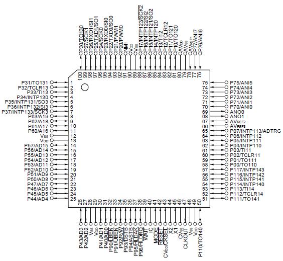
Pinout

  Connection Diagram


Specifications

Parameter Symbol Conditions   Ratings Unit
Power supply voltage VDD VDD pin 0.5 to +7.0 V
CVDD CVDD pin 0.5 to VDD + 0.3 V
CVSS CVSS pin 0.5 to +0.5 V
AVDD AVDD pin 0.5 to VDD + 0.3 V
AVSS AVSS pin 0.5 to +0.5 V
Input voltage VI1 Note, VDD = 5.0 V ±10% 0.5 to VDD + 0.3 V
Clock input voltage VK X1 pin, VDD = 5.0 V ±10% 0.5 to VDD + 1.0 V
Output current, low IOL Per pin 4.0 mA
Total for all pins 100 mA
Output current, high IOH Per pin 4.0 mA
    Total for all pins 100 mA
Output voltage VO VDD = 5.0 V ±10% 0.5 to VDD + 0.3 V
Analog input voltage VIAN P70/ANI0 to P77/ANI7 AVDD > VDD 0.5 to VDD + 0.3 V
VDDAVDD 0.5 to AVDD + 0.3 V
Analog reference input voltage AVREF AVREF1 to AVREF3 AVDD > VDD 0.5 to VDD + 0.3 V
VDDAVDD 0.5 to AVDD + 0.3 V
Operating ambient temperature TA     40 to +85 °C
Storage temperature Tstg     65 to +150  


Customers Who Bought This Item Also Bought

Margin,quality,low-cost products with low minimum orders. Secure your online payments with SeekIC Buyer Protection.
Transformers
Integrated Circuits (ICs)
RF and RFID
Semiconductor Modules
Resistors
Connectors, Interconnects
View more