70F3017AY

Features: . Number of instructions: 74. Minimum instruction execution time: 59 ns (@ 17 MHz operation with main systemclock (fXX)) 50 ns (@ 20 MHz operation with main systemclock (fXX)) 30.5 Ps (@ 32.768 kHz operation with subsystemclock (fXT)). General-purpose registers: 32 bits u32 registers. In...

product image

70F3017AY Picture
SeekIC No. : 004240213 Detail

70F3017AY: Features: . Number of instructions: 74. Minimum instruction execution time: 59 ns (@ 17 MHz operation with main systemclock (fXX)) 50 ns (@ 20 MHz operation with main systemclock (fXX)) 30.5 Ps (@ 3...

floor Price/Ceiling Price

Part Number:
70F3017AY
Supply Ability:
5000

Price Break

  • Qty
  • 1~5000
  • Unit Price
  • Negotiable
  • Processing time
  • 15 Days
Total Cost: $ 0.00

SeekIC Buyer Protection PLUS - newly updated for 2013!

  • Escrow Protection.
  • Guaranteed refunds.
  • Secure payments.
  • Learn more >>

Month Sales

268 Transactions

Rating

evaluate  (4.8 stars)

Upload time: 2024/4/27

Payment Methods

All payment methods are secure and covered by SeekIC Buyer Protection PLUS.

Notice: When you place an order, your payment is made to SeekIC and not to your seller. SeekIC only pays the seller after confirming you have received your order. We will also never share your payment details with your seller.
Product Details

Description


Features:

. Number of instructions:  74
. Minimum instruction execution time:
  59 ns (@ 17 MHz operation with main systemclock (fXX))
  50 ns (@ 20 MHz operation with main systemclock (fXX))
  30.5 Ps (@ 32.768 kHz operation with subsystemclock (fXT))
. General-purpose registers:  32 bits u 32 registers
. Instruction set:
  Signed multiplication, saturation operations, 32-bit
  shift instructions, bit manipulation instructions,
  load/store instructions
. Memory space:
  16 MB linear address space
  Memory block division function:  2 MB per block
. External bus interface:  16-bit data bus
  Address bus:  Separate output enabled
. Internal memory
  Flash memory:  256 KB
   RAM:  8 KB
. Interrupts and exceptions
  External:  8, internal:  23, exceptions: 1
. I/O lines  Total:  85
. Timer/counters
  16-bit timer:2 channels
  8-bit timer:4 channels
. Watch timer:  1 channel
. Watchdog timer:  1 channel
. Serial interface (SIO)
  Asynchronous serial interface (UART)
  Clocked serial interface (CSI)
  I2C bus interface (PPD70F3017AY)
. A/D converter:  12 channels
. DMA controller:  3 channels
. RTP:  8 bits u1 channel or 4 bits u 2 channels
. Power-saving functions: HALT/IDLE/STOP modes
. Packages:100-pin plastic LQFP (14 u 14 mm)
                  121-pin plastic FBGA (12 u 12 mm)


Application

*Low-power portable devices
*Cellular phones, PHSs, and camcorders


Pinout

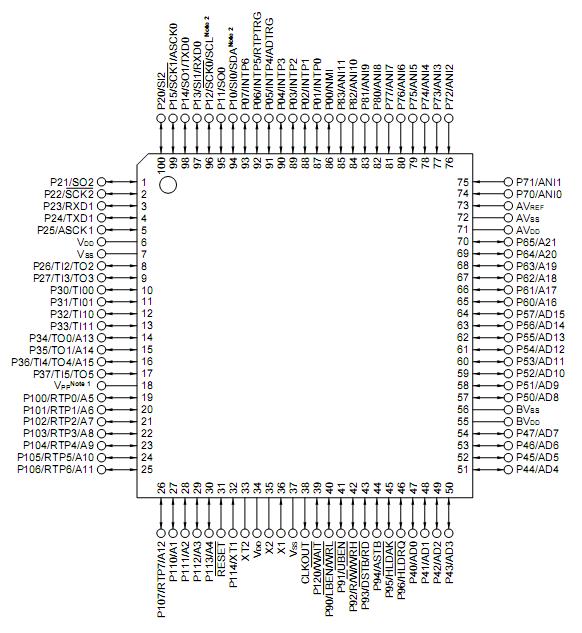
  Connection Diagram


Specifications

Parameter

Symbol

Conditions

Ratings

Unit

Supply voltage

VDD


0.5 to +4.6

V

VPP


0.5 to +8.5

V

AVDD


0.5 to +4.6

V

BVDD


0.5 to +4.6

V

VSS


0.5 to +0.5

V

AVSS


0.5 to +0.5

V

BVSS


0.5 to +0.5

V

Input voltage

VI1

Note 1, P114,RESET

0.5 to VDD+ 0.5Note 4

V

VI2

Note 2

0.5 to BVDD+ 0.5Note 4

V

Clock input voltage

VK

X1, XT1, XT2, VDD= 2.7 to 3.6 V

0.5 to VDD+ 1.0Note 4

V

Analog input voltage

VIAN

Note 3(AVDD)

0.5 to AVDD+ 0.5Note 4

V

Analog reference inputvoltage

AVREF

AVREF

0.5 to AVDD+ 0.5Note 4

V

Output current, low

IOL

Per pin

4.0

mA

Total for P00 to P07, P10 to P15, P20 to P25

25

mA

Total for P26, P27, P30 to P37, P100 toP107, P110 to P113

25

mA

Total for P40 to P47, P90 to P96, P120,CLKOUT

25

mA

Total for P50 to P57, P60 to P65

25

mA

Output current, high

IOH

Per pin

4.0

mA

Total for P00 to P07, P10 to P15, P20 to P25

25

mA

Total for P26, P27, P30 to P37, P100 toP107, P110 to P113

25

mA

Total for P40 to P47, P90 to P96, P120,CLKOUT

25

mA

Total for P50 to P57, P60 to P65

25

mA

Output voltage

VO1

Note 1, VDD= 2.7 to 3.6 V

0.5 to VDD+ 0.5Note 4

V

VO2

Note 2, CLKOUT, BVDD= 2.7 to 3.6 V

0.5 to BVDD+ 0.5Note 4

V

Operating ambient temperature

TA

Normal operating mode

40 to +85

°C

Flash memory programming mode

10 to 40

°C

Storage temperature

Tstg


40 to +125

°C


Description

The µPD70F3015B, 70F3015BY, 70F3017A, and 70F3017AY are products with on-chip flash memory.  Becausethe devices can be programmed by the user on-board, they are ideal for the evaluation stages of systemdevelopment, small-scale production of a variety of products, and rapiddevelopment of new products.

The 70F3017AY provides a high-level cost performance ideal for applications ranging from low-power camcordersand other AV equipment to portable telephone equipment such as cellular phones and personal handyphonesystems (PHS).

Detailed function descriptions of 70F3017AY are provided in the following user's manuals.  Be sure to read them beforedesigning.
V850/SA1 User's Manual  Hardware:U12768E
V850 FamilyTM User's Manual  Architecture:U10243E


Customers Who Bought This Item Also Bought

Margin,quality,low-cost products with low minimum orders. Secure your online payments with SeekIC Buyer Protection.
Semiconductor Modules
Cables, Wires
Computers, Office - Components, Accessories
View more