Mounting Style
: SMD/SMT
Supply Voltage - Max
: 5.5 V
Polarity
: Non-Inverting
Input Type
: Single-Ended
Output Type
: Single-Ended
Maximum Operating Temperature
: + 85 C
Package / Case
: SOP-20
Packaging
: Tube
Number of Circuits
: 8
Logic Type
: D-Type Flip-Flop
High Level Output Current
: - 32 mA
Low Level Output Current
: 64 mA
Propagation Delay Time
: 6.8 ns
Logic Family
: 74ABT
Features: Clock enable for address and data synchronization applications
Eight edge-triggered D-type flip-flops
Buffered common clock
See ABT273 for master reset version
See ABT373 for transparent latch version
See ABT374 for 3-STATE version
Output sink capability of 64 mA, source capability of 32 mA
Guaranteed latchup protection
High impedance glitch free bus loading during entire power up and power down cycle
Non-destructive hot insertion capability
Disable time less than enable time to avoid bus contentionPinout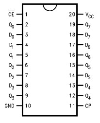 SpecificationsStorage Temperature........................ −65°C to +150°C
Ambient Temperature under Bias...... −55°C to +125°C
Junction Temperature under Bias...... −55°C to +150°C
VCC Pin Potential to Ground Pin .............−0.5V to +7.0V
Input Voltage (Note 2) ..........................−0.5V to +7.0V
Input Current (Note 2) ....................−30 mA to +5.0 mA
Voltage Applied to Any Output
in the Disabled or
Power-OFF State............................. −0.5V to +4.75V
in the HIGH State ..................................−0.5V to VCC
Current Applied to Output
in LOW State (Max)............. Twice the rated IOL (mA)
DC Latchup Source Current............................. −500 mA
(Across Comm Operating Range)
Over Voltage Latchup ...................................VCC + 4.5VDescriptionThe 74ABT377CSJ has eight edge-triggered, D-type flip-flops with individual D inputs and Q outputs. The common buffered Clock (CP) input loads all flip-flops simultaneously when the Clock Enable (CE) is LOW.
The register is fully edge-triggered. The state of each D input, one setup time before the LOW-to-HIGH clock transition, is transferred to the corresponding flip-flop's Q output. The CE input must be stable only one setup time prior to the LOW-to-HIGH clock transition for predictable operation.
 74ABT377CSJ Data Sheet