Features: Inputs Are TTL-Voltage CompatibleCombines '244 and '280 Functions In One PackageFlow-Through Architecture Optimizes PCB LayoutCenter-Pin VCC and GND Configurations Minimize High-Speed Switching NoiseEPICTM (Enhanced-Performance Implanted CMOS) 1-mm Process500-mA Typical Latch-Up Immunity...
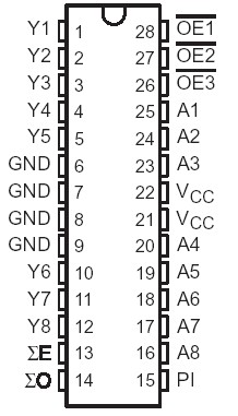
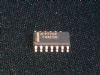
74ACT11656: Features: Inputs Are TTL-Voltage CompatibleCombines '244 and '280 Functions In One PackageFlow-Through Architecture Optimizes PCB LayoutCenter-Pin VCC and GND Configurations Minimize High-Speed Swit...
SeekIC Buyer Protection PLUS - newly updated for 2013!
268 Transactions
All payment methods are secure and covered by SeekIC Buyer Protection PLUS.
The 74ACT11656 contains eight noninverting buffers with 3-state outputs and a 9-bit parity generator/checker. The device is intended for bus-oriented applications.
When data is transmitted, the parity input (PI) terminal is configured as an input and combined with the A-input data to generate a flag on either parity output (SE or SO) terminal, depending on the number of inputs that are high.
The output-enable (OE1, OE2, and OE3) inputs can be used to disable the device so that the buses are effectively isolated.
The 74ACT11656 is characterized for operation from 40°C to 85°C.
The 74ACT11656 is designed as octal buffer and line driver which contains eight noninverting buffers with 3-state outputs and a 9-bit parity generator/checker. The device is intended for bus-oriented applications.
It has six features. (1)Inputs are TTL-voltage compatible. (2)Combines '244 and '280 functions in one package. (3)Flow-through architecture optimizes PCB layout. (4)Center-pin Vcc and GND configurations minimize high-speed switching noise. (5)EPIC enhanced-performance implanted CMOS) 1mm process. (6)500mA typical latch-up immunity at 125°C. Those are all the main features.
Some absolute maximum ratings of the 74ACT11656 have been concluded into several points as follow. (1)Its supply voltage would be from -0.5V to 7V. (2)Its input voltage range would be from -0.5V to Vcc+0.5V. (3)Its output voltage range would be from -0.5V to Vcc+0.5V. (4)Its input clamp current would be ±20mA. (5)Its output clamp current would be ±50mA. (6)Its continuous output current would be ±50mA. (7)Its continuous current through Vcc or GND would be from ±225mA. (8)Its maximum power dissipation at Ta=55°C (in still air) would be 1.7W. (9)Its operating free-air temperature range would be from -40° C to 85°C. (10)Its storage temperature range would be from -65° C to 150°C. It should be noted that stresses above those listed in absolute maximum ratings may cause permanent damage to device.
Also some electrical characteristics of the 74ACT11656 are concluded as follow. (1)Its output voltage high would be min 4.4V. (2)Its output voltage low would be max 0.1V. (3)Its input current would be max +/-1uA. (4)Its high-impedance-state output current would be max +/-0.5uA. (5)Iys supply current would be max 8uA. (6)Its input capacitance would be typ 4.5pF. (7)Its output capacitance would be typ 10pF. (8)Its power dissipation capacitance per buffer would be typ 70pF for outputs enabled and would be typ 22pF for outputs disabled. And so on. If you have any question or suggestion or want to know more information please contact us for details. Thank you!