Features: • Inputs Are TTL-Voltage Compatible
• Flow-Through Architecture Optimizes PCB Layout
• Center-Pin VCC and GND Pin Configurations Minimize High-Speed Switching Noise
• EPICE (Enhanced-Performance Implanted CMOS) 1-mm Process
• 500-mA Typical Latch-Up Immunity at 125°C
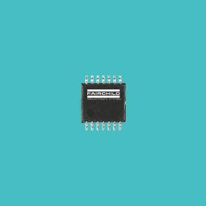
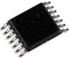
• Package Options Include Plastic Small-Outline Packages and Standard Plastic 300-mil DIPsPinout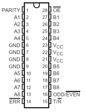 Specifications
Supply voltage range, VCC . . . . . . . . . . . . . . . . . . . . . . . . . . . . . . . . . . . . . . . . . . . . .0.5 V to 7 V
Input voltage range, VI (see Note 1) . . . . . . . . . . . . . . . . . . . . . . . . . . .. . . . .0.5 V to VCC + 0.5 V
Output voltage range, VO (see Note 1) . . . . . . . . . . . . . . . . . . . . . . . . . . . . . .0.5 V to VCC + 0.5 V
Input clamp current, IIK (VI < 0 or VI > VCC) . . . . . . . . . . . . . . . . . . . . . . . . . . . .. . . . . . . . . .±20 mA
Output clamp current, IOK (VO < 0 or VO > VCC) . . . . . . . . . . . . . . . . . . . . . . . . . . . . . . . . . . ±50 mA
Continuous output current, IO (VO = 0 to VCC) . . . . . . . . . . . . . . . . . . . . . . . . . . . . .. . . . . . .±50 mA
Continuous current through VCC or GND . . . . . . . . . . . . . . . . . . . . . . . . . . . . . . . . . . . . . . .±225 mA
Storage temperature range . . . . . . . . . . . . . . . . . . . . . . . . . . . . . . . . . . .. . . . . . . . .65°C to 150°C
DescriptionThe 74ACT11657 contains eight noninverting buffers with 3-state outputs and an 8-bit parity generator/checker and is intended for busoriented applications.
The transmit/receive (T/R) input determines the direction of data flow through the bidirectional transceivers. When T/R is high, data flows from the A port to the B port (transmit mode); when T/R is low, data flows from the B port to the A port (receive mode). When the output-enable (OE) input is high, both the A and B ports are in the high-impedance state.
Odd or even parity of the 74ACT11657 is selected by a logic high or low level, respectively, on the ODD/EVEN input. PARITY carries the parity bit value; it is an output from the parity generator/checker in the transmit mode and an input to the parity generator/checker in the receive mode.
In the transmit mode, after the A bus is polled to determine the number of high bits, PARITY is set to the logic level that maintains the parity sense selected by the level at the ODD/EVEN input. For example, if ODD/EVEN is low (even parity selected) and there are five high bits on the A bus, then PARITY is set to the logic high level so that an even number of the nine total bits (eight A-bus bits plus parity bit) are high.
In the receive mode of the 74ACT11657, after the B bus is polled to determine the number of high bits, the ERR output logic level indicates whether or not the data to be received exhibits the correct parity sense. For example, if ODD/EVEN is high (odd parity selected), PARITY is high, and there are three high bits on the B bus, then ERR is low, indicating a parity error.
The 74ACT11657 is characterized for operation from 40°C to 85°C.

 74ACT11657 Data Sheet