74ACT18825

Features: · Broadside pinout allows for easy board layout· Separate control logic for each byte· Extra data width for wider address/data paths or buses carrying parity· Outputs source/sink 24 mA· TTL-compatible inputsPinoutSpecificationsSupply Voltage (VCC) ...........................-0.5V to +7.0...

product image

74ACT18825 Picture
SeekIC No. : 004249048 Detail

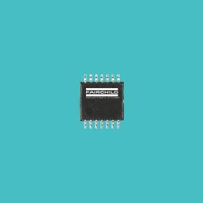
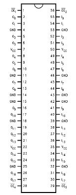
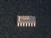
74ACT18825: Features: · Broadside pinout allows for easy board layout· Separate control logic for each byte· Extra data width for wider address/data paths or buses carrying parity· Outputs source/sink 24 mA· TT...

floor Price/Ceiling Price

Part Number:
74ACT18825
Supply Ability:
5000

Price Break

  • Qty
  • 1~5000
  • Unit Price
  • Negotiable
  • Processing time
  • 15 Days
Total Cost: $ 0.00

SeekIC Buyer Protection PLUS - newly updated for 2013!

  • Escrow Protection.
  • Guaranteed refunds.
  • Secure payments.
  • Learn more >>

Month Sales

268 Transactions

Rating

evaluate  (4.8 stars)

Upload time: 2024/4/29

Payment Methods

All payment methods are secure and covered by SeekIC Buyer Protection PLUS.

Notice: When you place an order, your payment is made to SeekIC and not to your seller. SeekIC only pays the seller after confirming you have received your order. We will also never share your payment details with your seller.
Product Details

Description


Features:

· Broadside pinout allows for easy board layout
· Separate control logic for each byte
· Extra data width for wider address/data paths or buses carrying parity
· Outputs source/sink 24 mA
· TTL-compatible inputs


Pinout

  Connection Diagram


Specifications

Supply Voltage (VCC) ...........................-0.5V to +7.0V
DC Input Diode Current (IIK)
VI = -0.5V ........................................................-20 mA
VI = VCC +0.5V.............................................. +20 mA
DC Output Diode Current (IOK)
VO = -0.5V...................................................... -20 mA
VO = VCC +0.5V............................................ +20 mA
DC Output Voltage (VO)............. -0.5V to VCC + 0.5V
DC Output Source/Sink Current (IO) ............±50 mA
DC VCC or Ground Current
Per Output Pin .............................................±50 mA
Storage Temperature.................. -65°C to +150°C


Description

The 74ACT18825 contains eighteen non-inverting buffers with 3-STATE outputs designed to be employed as a memoryand address driver, clock driver, or bus oriented transmitter/receiver. The device is byte controlled. Each byte has separate 3-STATE control inputs which can be shorted together for full 18-bit operation.


Customers Who Bought This Item Also Bought

Margin,quality,low-cost products with low minimum orders. Secure your online payments with SeekIC Buyer Protection.
RF and RFID
Crystals and Oscillators
Power Supplies - Board Mount
Connectors, Interconnects
Resistors
View more