Number of Circuits
: 1
Maximum Operating Temperature
: + 125 C
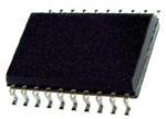
Mounting Style
: SMD/SMT
Supply Voltage - Max
: 5.5 V
Polarity
: Non-Inverting
Input Type
: Single-Ended
Output Type
: Single-Ended
Packaging
: Tube
Low Level Output Current
: 8 mA
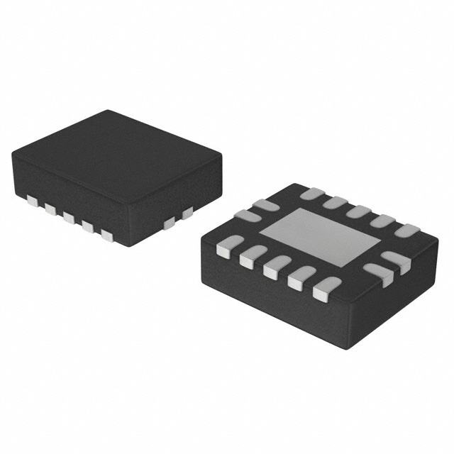
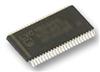
Package / Case
: SOT-163
Logic Type
: D-Type Edge Triggered Flip-Flop
High Level Output Current
: - 8 mA
Logic Family
: AHC
Propagation Delay Time
: 4.4 ns at 5 V
DescriptionThe 74AHC374D belongs to 74AHC/AHCT374 family which are high-speed Si-gate CMOS devices and are pin compatible with low power Schottky TTL (LSTTL). The 8 flip-flops will store the state of their individual D-inputs that meet the set-up and hold times requirements on the LOW-to-HIGH CP transition. When OE is LOW the contents of the 8 flip-flops are available at the outputs. When OE is HIGH, the outputs go to the high-impedance OFF-state. Operation of the OE input does not affect the state of the flip-flops. The '374' is functionally identical to the '534', but has non-inverting outputs. They are specified in compliance with JEDEC standard No. 7A. The 74AHC374D are octal D-type flip-flops featuring separate D-type inputs for each flip-flop and 3-state outputs for bus oriented applications. A clock (CP) and an output enable (OE) input are common to all flip-flops.
The features of 74AHC374D can be summarized as (1)ESD protection: HBM EIA/JESD22-A114-A exceeds 2000 V, MM EIA/JESD22-A115-A exceeds 200 V, CDM EIA/JESD22-C101 exceeds 1000 V; (2)balanced propagation delays; (3)all inputs of the 74AHC374D have schmitt-trigger actions; (4)inputs accepts voltages higher than VCC; (5)common 3-state output enable input; (6)ICC category: MSI; (7)for AHC only: operates with CMOS input levels; (8)for AHCT only: operates with TTL input levels; (9)specified from -40 to +85 and +125 °C.
The absolute maximum ratings of 74AHC374D are (1)VCC DC supply voltage: -0.5 to +7.0V; (2)VI input voltage range: -0.5 to +7.0V; (3)IIK DC input diode current(VI < -0.5 V; note 1): -20mA; (4)IOK DC output diode current(VO < -0.5 V or VO > VCC + 0.5 V; note 1): ±20mA; (5)IO DC output source or sink current(-0.5 V < VO < VCC + 0.5 V): ±25 mA; (6)ICC DC VCC or GND current: ±75mA; (7)Tstg storage temperature range: -65 to +150°C; (8)PD power dissipation per package(for temperature range: -40 to +125 °C; note 2): 500mW(1. The input and output voltage ratings of the 74AHC374D may be exceeded if the input and output current ratings are observed. 2. For SO packages: above 70 °C the value of PD derates linearly with 8 mW/K. For TSSOP packages: above 60 °C the value of PD derates linearly with 5.5 mW/K.)
 74AHC374D Data Sheet