74HC195

Features: · Asynchronous master reset· J, K, (D) inputs to the first stage· Fully synchronous serial or parallel data transfer· Shift right and parallel load capability· Complement output from the last stage· Output capability: standard· ICC category: MSIApplication· Serial data transfer· Parallel...

product image

74HC195 Picture
SeekIC No. : 004250710 Detail

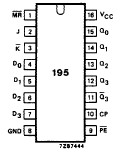
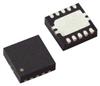
74HC195: Features: · Asynchronous master reset· J, K, (D) inputs to the first stage· Fully synchronous serial or parallel data transfer· Shift right and parallel load capability· Complement output from the l...

floor Price/Ceiling Price

Part Number:
74HC195
Supply Ability:
5000

Price Break

  • Qty
  • 1~5000
  • Unit Price
  • Negotiable
  • Processing time
  • 15 Days
Total Cost: $ 0.00

SeekIC Buyer Protection PLUS - newly updated for 2013!

  • Escrow Protection.
  • Guaranteed refunds.
  • Secure payments.
  • Learn more >>

Month Sales

268 Transactions

Rating

evaluate  (4.8 stars)

Upload time: 2024/4/28

Payment Methods

All payment methods are secure and covered by SeekIC Buyer Protection PLUS.

Notice: When you place an order, your payment is made to SeekIC and not to your seller. SeekIC only pays the seller after confirming you have received your order. We will also never share your payment details with your seller.
Product Details

Description


Features:

· Asynchronous master reset
· J, K, (D) inputs to the first stage
· Fully synchronous serial or parallel data transfer
· Shift right and parallel load capability
· Complement output from the last stage
· Output capability: standard
· ICC category: MSI


Application

· Serial data transfer
· Parallel data transfer
· Serial-to-parallel data transfer
· Parallel-to-serial data transfer


Pinout

  Connection Diagram


Description

The 74HC195 is high-speed Si-gate CMOS devices and are pin compatible with low power Schottky TTL (LSTTL). They are specified in compliance with JEDEC standard no. 7A.

The 74HC195 performs serial, parallel, serial-to-parallel or parallel-to-serial data transfer at very high speeds. The "195" operates on two primary modes:shift right (QoQ1) and parallel load, which are controlled by the state of the parallel load enable (PE) input. Serial data enters the first flip-flop (Q0) via the J and K inputs when the PE input is HIGH and shifted one bit in the direction Q0Q1 Q2  Q3 following each LOW-to-HIGH clock transition. The J and K inputs provide the flexibility of the JK type input of the 74HC195 for special applications and by tying the pins together, the simple D-type input for general applications. The "195" appears as four common clocked D flip-flops when the PE input is LOW.

After the LOW-to-HIGH clock transition, data on the parallel inputs (D0 to D3) is transferred to the respective Q0 to Q3 outputs. Shift left operation (Q Q2) can be achieved by tying the Qn outputs to the Dn-1 inputs and holding the PE input LOW.

All parallel and serial data transfers of the 74HC195 are synchronous, occurring after each LOW-to-HIGH clock transition. There is no restriction on the activity of the J, K, Dn and PE inputs for logic operation other than the set-up and hold time requirements. A LOW on the asynchronous master reset (MR) input sets all Q outputs LOW, independent of any other input condition.


Customers Who Bought This Item Also Bought

Margin,quality,low-cost products with low minimum orders. Secure your online payments with SeekIC Buyer Protection.
Sensors, Transducers
Computers, Office - Components, Accessories
Static Control, ESD, Clean Room Products
Semiconductor Modules
Fans, Thermal Management
Inductors, Coils, Chokes
View more